System Control Coprocessor
ARM DDI 0363E
Copyright © 2009 ARM Limited. All rights reserved.
4-41
ID013010
Non-Confidential, Unrestricted Access
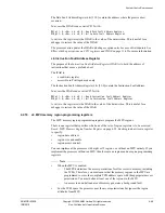
To access the Auxiliary Control Register, read or write CP15 with:
MRC p15, 0, <Rd>, c1, c0, 1 ; Read Auxiliary Control Register
MCR p15, 0, <Rd>, c1, c0, 1 ; Write Auxiliary Control Register
ARM recommends that any instruction that changes bits [31:28] or [7] is followed by an
ISB
instruction to ensure that the changes have taken effect before any dependent instructions are
executed.
c15, Secondary Auxiliary Control Register
The Secondary Auxiliary Control Register is:
•
a read/write register
•
accessible in Privileged mode only.
Note
This register is implemented from the r1p
m
releases of the processor. Attempting to access this
register in r0p
m
releases of the processor results in an Undefined Instruction exception.
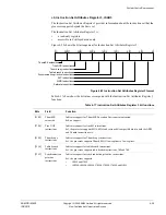
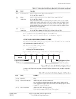
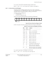
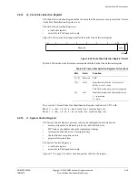
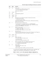
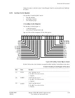
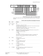
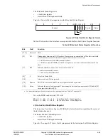
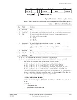
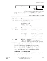
Figure 4-29 on page 4-42 shows the arrangement of bits in the register.
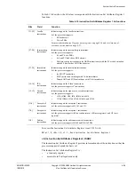
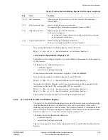
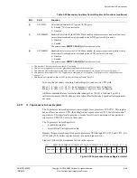
[2]
B1TCMECEN
B1TCM external error enable:
0 = Disabled
1 = Enabled.
The primary input
ERRENRAM[2]
defines the reset value.
[1]
B0TCMECEN
B0TCM external error enable:
0 = Disabled
1 = Enabled.
The primary input
ERRENRAM[1]
defines the reset value.
[0]
ATCMECEN
ATCM external error enable:
0 = Disabled
1 = Enabled.
The primary input
ERRENRAM[0]
defines the reset value.
a. See
Dual issue
on page 14-34
b. See
Configuration signals
on page A-4.
c. This bit is only supported if parity error generation is implemented in your design.
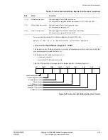
Table 4-24 Auxiliary Control Register bit functions (continued)
Bits
Field Function

