System Control Coprocessor
ARM DDI 0363E
Copyright © 2009 ARM Limited. All rights reserved.
4-59
ID013010
Non-Confidential, Unrestricted Access
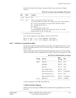
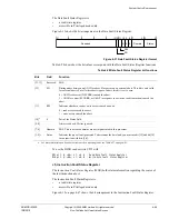
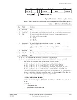
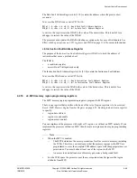
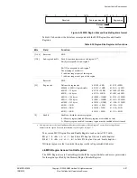
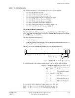
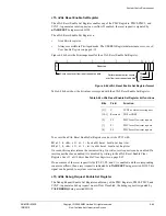
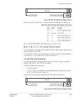
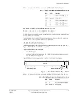
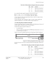
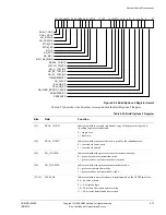
Figure 4-42 ATCM Region Registers
Table 4-40 shows how the bit values correspond with the ATCM Region Register.
To access the ATCM Region Register, read or write CP15 with:
MRC p15, 0, <Rd>, c9, c1, 1
; Read ATCM Region Register
MCR p15, 0, <Rd>, c9, c1, 1
; Write ATCM Region Register
4.2.23
c9, TCM Selection Register
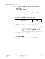
The TCM Selection Register determines the TCM region register that the processor writes to.
The processor only supports one TCM region for each TCM interface, and the TCM Selection
Register Reads-As-Zero and ignores writes. It is only accessible in Privileged mode.
4.2.24
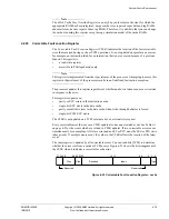
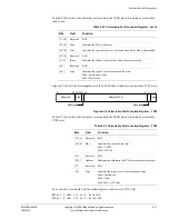
c11, Slave Port Control Register
The Slave Port Control Register enables or disables TCM access to the AXI slave port in
Privileged or User mode.
Note
Use the Auxiliary Control Register to enable access to the cache RAMs through the AXI slave
port. See
Auxiliary Control Registers
on page 4-38.
Base address
31
12 11
7 6
2 1 0
Reserved
Size
Reserved
Enable
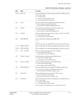
Table 4-40 ATCM Region Register bit functions
Bits
Field
Function
[31:12] Base
address
Base address. Defines the base address of the ATCM. The base address must be aligned to the
size of the ATCM. Any bits in the range [(log
2
(RAMSize)-1):12] are ignored.
At reset, if
LOCZRAMA
is set to:
0 = The initial base address is implementation-defined. See
Configurable options
on page 1-13
1 = The initial base address is
0x0
.
[11:7]
Reserved
UNP on reads, SBZ on writes.
[6:2]
Size
Size. Indicates the size of the ATCM on reads. On writes this field is ignored. See
About the TCMs
on page 8-13.
b00000 = 0KB
b00011 = 4KB
b00100 = 8KB
b00101 = 16KB
b00110 = 32KB
b00111 = 64KB
b01000 = 128KB
b01001 = 256KB
b01010 = 512kB
b01011 = 1MB
b01100 = 2MB
b01101 = 4MB
b01110 = 8MB.
[1]
Reserved
SBZ
[0]
Enable
Enables or disables the ATCM.
0 = Disabled
1 = Enabled. The reset value of this field is determined by the
INITRAMA
input pin.

