Level Two Interface
ARM DDI 0363E
Copyright © 2009 ARM Limited. All rights reserved.
9-20
ID013010
Non-Confidential, Unrestricted Access
9.4
AXI slave interface
The processor has a single AXI slave interface, with one port. The port is 64 bits wide and
conforms to the AXI standard as described in the
AMBA AXI Protocol Specification
. Within the
AXI standard, the slave port uses the
AWUSERS
and
ARUSERS
each as four separate chip
select input signals to enable access to:
•
BTCM
•
ATCM
•
instruction cache RAMs
•
data cache RAMs.
The external AXI system must generate the chip select signals. The slave interface routes the
access to the required RAM.
In addition, the AXI slave interface produces or checks parity bits for each AXI channel. These
additional signals are not part of the AXI specification. See the
Cortex-R4 and Cortex-R4F
Integration Manual
for more information.
The slave interface can run at the same frequency as the processor or at a lower, synchronous
frequency. See
AXI interface clocking
on page 3-9 for more information. If asynchronous
clocking is required an external asynchronous AXI register slice is required.
The AXI slave provides access to the TCMs and competes for access to the TCMs with the LSU
and PFU. Both the LSU and PFU normally have a higher priority than the AXI slave.
If two BTCM ports are used, you can configure these to interleave in the address map, so any
AXI slave access that is denied access to the BTCM on the first cycle of the access gains access
on the second cycle when the LSU is using the other port, and can continue in lock-step with the
LSU, assuming both are accessing sequential data. Accesses to the ATCM are more likely to
encounter a conflict because there is only one port on the interface.
Memory BIST ports are routed through the AXI slave interface logic, to access the RAMs.
Memory BIST access is assumed only to occur when no other accesses are taking place, and
takes highest priority.
9.4.1
AXI slave interface for cache RAMs
You can use the AXI slave for software testing of the cache RAMs in functional mode. When
the AXI slave is enabled to access the RAMs, the processor considers the caches as cache-off,
so that the instruction and data requests cannot interact with AXI slave requests. AXI slave
requests access the cache RAMs. Instruction and data requests are considered as Non-cacheable
and do not perform any lookup in the caches.
The AXI slave interface accesses each cache RAM individually.
On the instruction cache side the AXI slave can access:
•
data cache RAMs, data and parity or ECC code bits
•
tag RAMs, tag and parity or ECC code bits.
On the data cache side, the AXI slave can access:
•
data cache RAMs, data and parity or ECC code bits
•
tag RAMs, tag and parity or ECC code bits
•
dirty RAM, dirty bit and attributes, and ECC code bits.
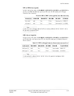
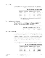
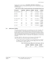
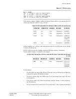
A simple decode of two address bits and four way address bits determines which of the data,
tag, or dirty RAMs is accessed within the caches. The AXI access is given a SLVERR error
response when access to nonexistent cache RAM is indicated.

