


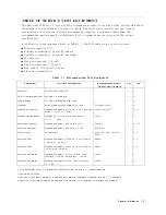


Required
Equipment
T
able
1-1
lists
the
equipment
required
to
perform
the
A
djustments
and
the
Correction
Constants
procedures
described
in
this
chapter
.
Use
only
calibrated
test
equipment
when
adjusting
the
analyzer
.
If
the
recommended
test
equipment
is
not
available
,
equipment
whose
specications
are
equal
to
,
or
surpasses
those
of
the
recommended
test
equipment
may
be
used.
W
arm-up
for
A
djustments
and
Correction
Constants
W
arm-up
the
analyzer
for
at
least
30
minute
before
performing
any
of
the
following
A
djustments
and
Correction
Constants
procedures
to
ensure
proper
results
and
correct
instrument
operation.
Instrument
Cover
Removal
T
o
gain
access
to
the
adjustment
components
,
you
need
to
remove
the
top
cover
and
the
side
covers
.
Order
Of
A
djustments
When
performing
more
than
one
A
djustments
or
Correction
Constants
procedure
,
perform
them
in
the
order
they
appear
in
this
chapter
.
The
procedures
are
presented
in
the
following
order:
40
MHz
Reference
Oscillator
Frequency
A
djustment
520
MHz
Level
A
djustment
CAL
OUT
Level
A
djustment
Comb
Generator
A
djustment
Step
Pretune
Correction
Constants
Second
Local
PLL
Lock
A
djustment
DC
Oset
and
Hold
Step
A
djustments
0
/90
Tracking
A
djustment
Band
P
ass
Filters
A
djustments
Final
Gain
A
djustment
Source
Mixer
Local
Leakage
A
djustment
RF
OUT
Level
Correction
Constants
Spectrum
Analyzer
Absolute
Magnitude
Correction
Constants
Network
Analyzer
Absolute
Magnitude
Correction
Constants
Crystal
Filter
Correction
Constants
IF
Gain
Errors
Correction
Constants
Network
Analyzer
Magnitude
Ratio/Phase
Correction
Constants
10
MHz
Reference
Oscillator
Frequency
A
djustment
(Option
1D5
Only)
2-2
Adjustments
and
Correction
Constants
Содержание Agilent 4396B
Страница 10: ......
Страница 32: ......
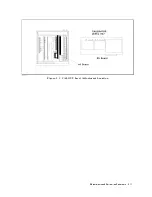
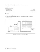
Страница 39: ...Figure 2 3 40 MHz Reference Oscillator Frequency Adjustment Location Adjustments and Correction Constants 2 7 ...
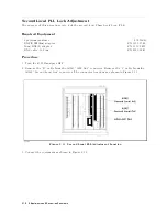
Страница 43: ...Figure 2 7 CAL OUT Level Adjustment Location Adjustments and Correction Constants 2 11 ...
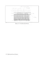
Страница 46: ...Figure 2 10 Comb Generator Output 2 14 Adjustments and Correction Constants ...
Страница 54: ...Figure 2 18 Plug Locations 19 Replace the A6 board into the slot 2 22 Adjustments and Correction Constants ...
Страница 62: ...Figure 2 26 Final Gain Adjustment Location 2 30 Adjustments and Correction Constants ...
Страница 70: ...Figure 2 34 IF Gain Errors Correction Constants Setup 2 2 38 Adjustments and Correction Constants ...
Страница 76: ...Figure 3 1 Troubleshooting Organization 3 2 T roubleshooting ...
Страница 84: ......
Страница 90: ...Figure 5 1 Power Supply Lines Simpli ed Block Diagram 5 2 Power Supply T roubleshooting ...
Страница 107: ...Figure 5 12 Power Supply Block Diagram 1 Power Supply T roubleshooting 5 19 ...
Страница 108: ...Figure 5 13 Power Supply Block Diagram 2 5 20 Power Supply T roubleshooting ...
Страница 109: ...Figure 5 14 Power Supply Block Diagram 3 Power Supply T roubleshooting 5 21 ...
Страница 110: ......
Страница 112: ...Figure 6 1 Digital Control Group Simpli ed Block Diagram 6 2 Digital Control T roubleshooting ...
Страница 124: ......
Страница 126: ...Figure 7 1 Source Group Block Diagram 7 2 Source Group T roubleshooting ...
Страница 160: ...Figure 8 1 Receiver Group Simpli ed Block Diagram 8 2 Receiver Group T roubleshooting ...
Страница 168: ......
Страница 184: ...Figure 10 6 External Test Setup 1 Figure 10 7 External Test Setup 2 10 10 Service Key Menus ...
Страница 185: ...Figure 10 8 External Test Setup 3 Figure 10 9 External Test Setup 4 Service Key Menus 10 11 ...
Страница 226: ...Figure 11 3 Power Supply Functional Group Simpli ed Block Diagram 11 6 Theory of Operation ...
Страница 231: ...Figure 11 5 Digital Control Group Simpli ed Block Diagram Theory of Operation 11 11 ...
Страница 235: ...Figure 11 6 Source Simpli ed Block Diagram Theory of Operation 11 15 ...
Страница 244: ...Figure 11 7 Receiver Simpli ed Block Diagram 11 24 Theory of Operation ...
Страница 249: ...Figure IDC5S11001 here Figure 11 8 4396B Source Group Block Diagram Theory of Operation 11 29 ...
Страница 250: ...Figure IDC5S11002 here Figure 11 9 4396B Receiver Group Block Diagram 11 30 Theory of Operation ...
Страница 254: ...Figure 12 1 Top View Major Assemblies 12 4 Replaceable Parts ...
Страница 290: ...Figure 12 36 Main Frame Assembly Parts 17 19 12 40 Replaceable Parts ...
Страница 294: ......
Страница 302: ...Figure B 1 Connector Locations On the A20 Motherboard Circuit Side B 2 A20 Motherboard Pin Assignment ...
Страница 303: ...Figure B 2 Pin Assignment On the A20 Motherboard Circuit Side A20 Motherboard Pin Assignment B 3 ...
Страница 308: ......
Страница 311: ...Figure C 1 Power Cable Supplied Power Requirement C 3 ...
Страница 312: ......
Страница 324: ......


