
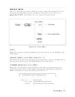


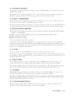


Figure
10-10.
External
T
est
Setup
5
17:
FRONT
P
ANEL
DIA
G.
Checks
the
RPG
and
all
front-panel
keys
on
the
A30
keyboard.
The
abbreviated
name
is
displayed
when
pressing
one
of
the
keys
or
rotating
the
RPG.
18:
DSK
DR
F
A
UL
T
ISOL'N
Checks
the
FDD
(Flexible
Disk
Drive).
When
this
test
is
started,
a
bit
pattern
is
written
to
the
exible
disk.
Then
the
pattern
is
read
back
and
checked.
This
write
pattern
check
is
repeated
from
the
low
to
high
addresses
.
Note
After
this
test
is
performed,
the
data
stored
on
the
oppy
disk
is
lost.
19:
PO
WER
SWEEP
LINEARITY
Checks
that
the
power
sweep
linearity
is
within
limits
.
As
a
result,
the
A3A1
ALC,
A3A2
2nd
LO
,
and
A3A3
are
veried.
External
test
setup
2
(shown
in
Figure
10-7)
is
used
in
this
test.
This
test
measures
the
RF
OUT
levels
in
the
power
sweep
mode
over
its
entire
span.
The
R
input
is
used
to
measure
the
RF
OUT
level.
20:
OUTPUT
A
TTENU
A
TOR
Checks
that
the
A7
attenuation
accuracy
relative
to
the
10
dB
setting
and
the
frequency
response
of
the
attenuation
are
within
limits
.
As
a
result,
the
A7
output
attenuator
is
veried.
External
test
setup
2
(shown
in
Figure
10-7)
is
used
in
this
test.
This
test
sets
the
output
attenuator
over
its
entire
setting
range
by
changing
the
RF
OUT
level.
F
or
each
setting,
the
RF
OUT
signal
level
is
measured
using
the
R
input
over
the
appropriate
frequency
range
.
10-12
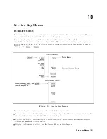
Service
K
ey
Menus
Содержание Agilent 4396B
Страница 10: ......
Страница 32: ......
Страница 39: ...Figure 2 3 40 MHz Reference Oscillator Frequency Adjustment Location Adjustments and Correction Constants 2 7 ...
Страница 43: ...Figure 2 7 CAL OUT Level Adjustment Location Adjustments and Correction Constants 2 11 ...
Страница 46: ...Figure 2 10 Comb Generator Output 2 14 Adjustments and Correction Constants ...
Страница 54: ...Figure 2 18 Plug Locations 19 Replace the A6 board into the slot 2 22 Adjustments and Correction Constants ...
Страница 62: ...Figure 2 26 Final Gain Adjustment Location 2 30 Adjustments and Correction Constants ...
Страница 70: ...Figure 2 34 IF Gain Errors Correction Constants Setup 2 2 38 Adjustments and Correction Constants ...
Страница 76: ...Figure 3 1 Troubleshooting Organization 3 2 T roubleshooting ...
Страница 84: ......
Страница 90: ...Figure 5 1 Power Supply Lines Simpli ed Block Diagram 5 2 Power Supply T roubleshooting ...
Страница 107: ...Figure 5 12 Power Supply Block Diagram 1 Power Supply T roubleshooting 5 19 ...
Страница 108: ...Figure 5 13 Power Supply Block Diagram 2 5 20 Power Supply T roubleshooting ...
Страница 109: ...Figure 5 14 Power Supply Block Diagram 3 Power Supply T roubleshooting 5 21 ...
Страница 110: ......
Страница 112: ...Figure 6 1 Digital Control Group Simpli ed Block Diagram 6 2 Digital Control T roubleshooting ...
Страница 124: ......
Страница 126: ...Figure 7 1 Source Group Block Diagram 7 2 Source Group T roubleshooting ...
Страница 160: ...Figure 8 1 Receiver Group Simpli ed Block Diagram 8 2 Receiver Group T roubleshooting ...
Страница 168: ......
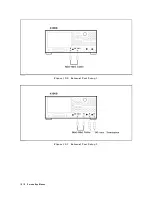
Страница 184: ...Figure 10 6 External Test Setup 1 Figure 10 7 External Test Setup 2 10 10 Service Key Menus ...
Страница 185: ...Figure 10 8 External Test Setup 3 Figure 10 9 External Test Setup 4 Service Key Menus 10 11 ...
Страница 226: ...Figure 11 3 Power Supply Functional Group Simpli ed Block Diagram 11 6 Theory of Operation ...
Страница 231: ...Figure 11 5 Digital Control Group Simpli ed Block Diagram Theory of Operation 11 11 ...
Страница 235: ...Figure 11 6 Source Simpli ed Block Diagram Theory of Operation 11 15 ...
Страница 244: ...Figure 11 7 Receiver Simpli ed Block Diagram 11 24 Theory of Operation ...
Страница 249: ...Figure IDC5S11001 here Figure 11 8 4396B Source Group Block Diagram Theory of Operation 11 29 ...
Страница 250: ...Figure IDC5S11002 here Figure 11 9 4396B Receiver Group Block Diagram 11 30 Theory of Operation ...
Страница 254: ...Figure 12 1 Top View Major Assemblies 12 4 Replaceable Parts ...
Страница 290: ...Figure 12 36 Main Frame Assembly Parts 17 19 12 40 Replaceable Parts ...
Страница 294: ......
Страница 302: ...Figure B 1 Connector Locations On the A20 Motherboard Circuit Side B 2 A20 Motherboard Pin Assignment ...
Страница 303: ...Figure B 2 Pin Assignment On the A20 Motherboard Circuit Side A20 Motherboard Pin Assignment B 3 ...
Страница 308: ......
Страница 311: ...Figure C 1 Power Cable Supplied Power Requirement C 3 ...
Страница 312: ......
Страница 324: ......


