


Line
P
ower
Module
The
line
power
module
includes
the
main
fuse
.
The
main
fuse
,
which
protects
the
input
side
of
the
preregulator
from
drawing
too
much
line
current,
is
also
accessible
at
the
rear
panel.
See
P
ower
R
equirements
in
appendix
C
for
the
fuse
replacement
and
other
power
considerations
.
A40
Preregulator
The
A40
preregulator
contains
a
rectier
and
a
switching
regulator
,
converts
the
line
voltage
to
+24
V
and
provides
it
to
the
A50
DC-DC
converter
.
A50
DC-DC
Converter
The
A50
DC-DC
Converter
consists
of
the
two
switching
regulators
(1
and
2).
The
DC-DC
convereter
provides
an
LED
(visible
at
the
top)
to
indicate
circuit
status
.
See
Figure
5-12
in
chapter
5.
The
shutdown
LED
is
turned
o
when
the
overcurrent
protection
circuit
activates
.
The
circuit
activates
when
an
overcurrent
is
sensed
on
the
+5
VD
power
line
,
when
an
overcurrent
is
sensed
on
the
four
power
supplies
(618
V
and
67.8
V),
or
when
the
F
AN
LOCK
signal
is
sensed.
It
shuts
down
the
ve
power
supplies
of
the
switching
regulators
(1
and
2).
F
or
A50
to
work
properly
,
the
+7.8
V
must
be
loaded
(approximately
680
ohms
,
more
than
125mW).
If
it
is
not,
the
other
preregulated
voltages
in
the
A50
DC-DC
converter
will
not
be
correct.
Switching
Regulator
1
Switching
regulator
1
converts
the
+24
V
to
the
regulated
+5
VD
(digital
supply).
The
+5
VD
goes
directly
to
the
A1
CPU
.
Switching
Regulator
2
Switching
preregulator
2
converts
the
+24
V
to
four
DC
voltages
,
+7.8
V
,
07.8
V
,
+18
V
,
018
V
.
The
voltages
are
routed
to
the
A2
post-regulator
for
nal
regulation.
Regulated
+5V
Digital
Supply
(+5
VD)
The
+5VD
power
supply
is
fully
regulated
in
the
A50
DC-DC
converter
.
It
goes
directly
to
the
A1
CPU
and
is
supplied
to
all
assemblies
requiring
a
digital
+5
V
supply
through
A1,
and
the
A20
motherboard.
See
Figure
11-3 .
A50
Shutdown
LED
The
A50
shutdown
LED
is
on
during
normal
operation.
It
turns
o
when
the
A50
protective
circuits
are
activated
and
shut
down
some
power
lines
.
The
shutdown
LED
turns
o
when
one
of
the
following
conditions
is
sensed:
Overcurrent
on
+5
VD
P
ower
Line
.
Overcurrent
on
the
four
power
supplies
(618
V
and
67.8
V)
F
an
is
not
rotating
(F
AN
LOCK
signal
is
sensed).
The
fan
obtains
its
power
+24
V
from
A40
preregulator
through
the
A50
DC-DC
converter
and
the
A2
post-regulator
.
When
the
power
is
missing,
the
F
AN
LOCK
signal
shuts
the
switching
regulators
down
and
turns
the
A50
shutdown
LED
o.
Theory
of
Operation
11-7
Содержание Agilent 4396B
Страница 10: ......
Страница 32: ......
Страница 39: ...Figure 2 3 40 MHz Reference Oscillator Frequency Adjustment Location Adjustments and Correction Constants 2 7 ...
Страница 43: ...Figure 2 7 CAL OUT Level Adjustment Location Adjustments and Correction Constants 2 11 ...
Страница 46: ...Figure 2 10 Comb Generator Output 2 14 Adjustments and Correction Constants ...
Страница 54: ...Figure 2 18 Plug Locations 19 Replace the A6 board into the slot 2 22 Adjustments and Correction Constants ...
Страница 62: ...Figure 2 26 Final Gain Adjustment Location 2 30 Adjustments and Correction Constants ...
Страница 70: ...Figure 2 34 IF Gain Errors Correction Constants Setup 2 2 38 Adjustments and Correction Constants ...
Страница 76: ...Figure 3 1 Troubleshooting Organization 3 2 T roubleshooting ...
Страница 84: ......
Страница 90: ...Figure 5 1 Power Supply Lines Simpli ed Block Diagram 5 2 Power Supply T roubleshooting ...
Страница 107: ...Figure 5 12 Power Supply Block Diagram 1 Power Supply T roubleshooting 5 19 ...
Страница 108: ...Figure 5 13 Power Supply Block Diagram 2 5 20 Power Supply T roubleshooting ...
Страница 109: ...Figure 5 14 Power Supply Block Diagram 3 Power Supply T roubleshooting 5 21 ...
Страница 110: ......
Страница 112: ...Figure 6 1 Digital Control Group Simpli ed Block Diagram 6 2 Digital Control T roubleshooting ...
Страница 124: ......
Страница 126: ...Figure 7 1 Source Group Block Diagram 7 2 Source Group T roubleshooting ...
Страница 160: ...Figure 8 1 Receiver Group Simpli ed Block Diagram 8 2 Receiver Group T roubleshooting ...
Страница 168: ......
Страница 184: ...Figure 10 6 External Test Setup 1 Figure 10 7 External Test Setup 2 10 10 Service Key Menus ...
Страница 185: ...Figure 10 8 External Test Setup 3 Figure 10 9 External Test Setup 4 Service Key Menus 10 11 ...
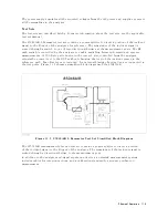
Страница 226: ...Figure 11 3 Power Supply Functional Group Simpli ed Block Diagram 11 6 Theory of Operation ...
Страница 231: ...Figure 11 5 Digital Control Group Simpli ed Block Diagram Theory of Operation 11 11 ...
Страница 235: ...Figure 11 6 Source Simpli ed Block Diagram Theory of Operation 11 15 ...
Страница 244: ...Figure 11 7 Receiver Simpli ed Block Diagram 11 24 Theory of Operation ...
Страница 249: ...Figure IDC5S11001 here Figure 11 8 4396B Source Group Block Diagram Theory of Operation 11 29 ...
Страница 250: ...Figure IDC5S11002 here Figure 11 9 4396B Receiver Group Block Diagram 11 30 Theory of Operation ...
Страница 254: ...Figure 12 1 Top View Major Assemblies 12 4 Replaceable Parts ...
Страница 290: ...Figure 12 36 Main Frame Assembly Parts 17 19 12 40 Replaceable Parts ...
Страница 294: ......
Страница 302: ...Figure B 1 Connector Locations On the A20 Motherboard Circuit Side B 2 A20 Motherboard Pin Assignment ...
Страница 303: ...Figure B 2 Pin Assignment On the A20 Motherboard Circuit Side A20 Motherboard Pin Assignment B 3 ...
Страница 308: ......
Страница 311: ...Figure C 1 Power Cable Supplied Power Requirement C 3 ...
Страница 312: ......
Страница 324: ......


