


CORRECTION
CONST
ANTS
MENU
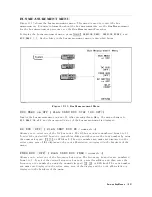
Figure
10-19
shows
the
correction
constants
menu.
This
menu
allows
you
to
turn
o
one
(or
more)
of
the
corrections
.
When
one
(or
more)
corrections
are
turned
o,
the
analyzer
displays
the
raw
measured
data.
Y
ou
can
check
the
raw
characteristics
of
the
source
and
receiver
circuit.
F
or
the
corrections
,
see
the
Correction
Constants.
T
o
display
the
menu,
press
4
System
5 ,
NNNNNNNNNNNNNNNNNNNNNNNNNNNNNNNNNNNNNN
SERVICE
MENU
,
NNNNNNNNNNNNNNNNNNNNNNNNNNNNNNNNNNNNNNNNN
SERVICE
MODES
,
and
NNNNNNNNNNNNNNNNNNNNNNNNNNNNNNNNNNNNNNNNNNNNNNNNNNNNNNNNNNNNNN
CORRECTION
CONSTANTS
.
Each
softkey
in
the
correction
constants
menu
is
described
below
.
Figure
10-19.
Correction
Constants
Menu
WWWWWWWWWWWWWWWWWWWWWWWWWWWWWWWWWWWWWWWWWWWWWWWWWWWWWWWWWWWWWWWWWWWWW
FRQ
RSP
CC
ON/off
(:DIAG:SERV:CCON:FRES
{OFF|ON|0|1}
)
T
oggles
the
receiver
frequency
response
correction
on
and
o.
When
the
correction
is
turned
o,
the
corrections
using
the
following
constants
are
turned
o.
Spectrum
analyzer
absolute
magnitude
correction
constants
.
Network
analyzer
absolute
magnitude
correction
constants
.
Network
analyzer
magnitude
ratio/phase
correction
constants
.
WWWWWWWWWWWWWWWWWWWWWWWWWWWWWWWWWWWWWWWWWWWWWWWWWWWWWWWWW
XTAL
CC
ON/off
(:DIAG:SERV:CCON:XTAL
{OFF|ON|0|1}
)
T
oggles
the
crystal
lter
frequency
response
correction
on
and
o.
When
this
correction
is
turned
o,
the
analyzer
does
not
perform
the
compensation
using
the
crystal
lter
correction
constants
.
10-32
Service
K
ey
Menus
Содержание Agilent 4396B
Страница 10: ......
Страница 32: ......
Страница 39: ...Figure 2 3 40 MHz Reference Oscillator Frequency Adjustment Location Adjustments and Correction Constants 2 7 ...
Страница 43: ...Figure 2 7 CAL OUT Level Adjustment Location Adjustments and Correction Constants 2 11 ...
Страница 46: ...Figure 2 10 Comb Generator Output 2 14 Adjustments and Correction Constants ...
Страница 54: ...Figure 2 18 Plug Locations 19 Replace the A6 board into the slot 2 22 Adjustments and Correction Constants ...
Страница 62: ...Figure 2 26 Final Gain Adjustment Location 2 30 Adjustments and Correction Constants ...
Страница 70: ...Figure 2 34 IF Gain Errors Correction Constants Setup 2 2 38 Adjustments and Correction Constants ...
Страница 76: ...Figure 3 1 Troubleshooting Organization 3 2 T roubleshooting ...
Страница 84: ......
Страница 90: ...Figure 5 1 Power Supply Lines Simpli ed Block Diagram 5 2 Power Supply T roubleshooting ...
Страница 107: ...Figure 5 12 Power Supply Block Diagram 1 Power Supply T roubleshooting 5 19 ...
Страница 108: ...Figure 5 13 Power Supply Block Diagram 2 5 20 Power Supply T roubleshooting ...
Страница 109: ...Figure 5 14 Power Supply Block Diagram 3 Power Supply T roubleshooting 5 21 ...
Страница 110: ......
Страница 112: ...Figure 6 1 Digital Control Group Simpli ed Block Diagram 6 2 Digital Control T roubleshooting ...
Страница 124: ......
Страница 126: ...Figure 7 1 Source Group Block Diagram 7 2 Source Group T roubleshooting ...
Страница 160: ...Figure 8 1 Receiver Group Simpli ed Block Diagram 8 2 Receiver Group T roubleshooting ...
Страница 168: ......
Страница 184: ...Figure 10 6 External Test Setup 1 Figure 10 7 External Test Setup 2 10 10 Service Key Menus ...
Страница 185: ...Figure 10 8 External Test Setup 3 Figure 10 9 External Test Setup 4 Service Key Menus 10 11 ...
Страница 226: ...Figure 11 3 Power Supply Functional Group Simpli ed Block Diagram 11 6 Theory of Operation ...
Страница 231: ...Figure 11 5 Digital Control Group Simpli ed Block Diagram Theory of Operation 11 11 ...
Страница 235: ...Figure 11 6 Source Simpli ed Block Diagram Theory of Operation 11 15 ...
Страница 244: ...Figure 11 7 Receiver Simpli ed Block Diagram 11 24 Theory of Operation ...
Страница 249: ...Figure IDC5S11001 here Figure 11 8 4396B Source Group Block Diagram Theory of Operation 11 29 ...
Страница 250: ...Figure IDC5S11002 here Figure 11 9 4396B Receiver Group Block Diagram 11 30 Theory of Operation ...
Страница 254: ...Figure 12 1 Top View Major Assemblies 12 4 Replaceable Parts ...
Страница 290: ...Figure 12 36 Main Frame Assembly Parts 17 19 12 40 Replaceable Parts ...
Страница 294: ......
Страница 302: ...Figure B 1 Connector Locations On the A20 Motherboard Circuit Side B 2 A20 Motherboard Pin Assignment ...
Страница 303: ...Figure B 2 Pin Assignment On the A20 Motherboard Circuit Side A20 Motherboard Pin Assignment B 3 ...
Страница 308: ......
Страница 311: ...Figure C 1 Power Cable Supplied Power Requirement C 3 ...
Страница 312: ......
Страница 324: ......


