


The
520
MHz
reference
signal
contains
40
MHz
harmonics
because
it
is
generated
by
multiplying
the
40
MHz
reference
signal
in
the
A5
synthesizer
.
The
Second
Local
PLL
A
djustment
adjusts
the
2nd
LO
to
lock
to
the
520
MHz
harmonic
,
rather
than
the
neighboring
harmonics
(480
MHz
or
560
MHz).
An
unlock
detector
monitors
the
control
voltage
to
the
V
CO
.
When
the
control
voltage
is
out
of
the
limits
,
the
detector
sends
the
status
to
the
A1
CPU
.
The
A1
CPU
causes
the
message
CA
UTION:
PHASE
LOCK
LOOP
UNLOCKED
to
be
displayed.
Source
First
Mixer
The
21.42
MHz
CW
signal
from
the
A3A1
ALC
is
mixed
with
the
2.08
GHz
second
local
oscillator
signal
through
the
rst
source
mixer
.
Then
the
signal
is
converted
to
a
2.05858
GHz
CW
signal
through
the
BPF
(band
pass
lter).
The
2.05858
GHz
signal
is
supplied
to
the
A3A3
source
.
A3A3
Source
The
A3A3
source
generates
a
stable
and
accurate
RF
signal.
This
signal
is
a
CW
or
swept
signal
between
100
kHz
to
1.8
GHz,
with
a
power
level
from
010
dBm
to
+20
dBm.
The
RF
signal
is
supplied
to
the
A7
output
attenuator
.
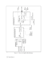
The
A3A3
source
consists
of
the
following
circuits
(see
Figure
11-6):
Source
Second
Mixer
Source
Amplier
Level
Detector
The
2.05858
GHz
IF
signal
from
the
A3A2
2nd
LO
is
applied
to
the
source
second
mixer
.
It
is
then
converted
to
the
CW
or
swept
RF
signal
(100
kHz
to
1.8
GHz)
by
mixing
with
the
CW
or
swept
1st
local
oscillator
signal
(2.05859
GHz
to
3.85858
GHz)
from
the
A4A1
1st
LO
.
The
RF
signal
is
amplied
with
a
constant
gain
through
the
source
amplier
.
It
is
then
supplied
to
the
A7
output
attenuator
through
the
level
detector
.
The
level
detector
loops
the
RF
signal
level
back
to
the
A3A1
ALC.
A7
Output
Attenuator
The
A7
output
attenuator
is
a
10
dB
step
attenuator
from
0
dB
to
60
dB
.
A7
consists
of
three
segments
(10
dB
,
20
dB
,
and
30
dB).
Attenuation
from
0
dB
to
60
dB
is
obtained
by
combining
one
(or
more)
of
the
three
segments
.
Each
segment
is
activated
by
the
TTL
signals
from
the
A2
post-regulator
.
The
TTL
signals
are
controlled
by
the
A1
CPU
.
The
RF
signal
from
the
A3A3
source
is
routed
to
the
front-panel
RF
OUT
connector
through
A7.
A7
is
used
to
produce
the
RF
OUT
power
range
of
060
dBm
to
20
dBm
using
the
A3A3
RF
signal
of
010
dBm
to
+20
dBm.
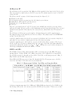
T
able
11-2
shows
the
relationship
between
the
RF
OUT
power
setting,
the
A3A3
output
level,
and
the
A7
setting
in
the
non-power
sweep
(frequency
sweep)
measurement.
The
RF
OUT
power
from
060
dBm
to
+10
dBm
is
obtained
by
attenuating
the
A3A3
RF
signal
of
0
dBm
to
+10
dBm.
This
reduces
errors
in
the
non
power
sweep
linearity
performance
due
to
the
ALC
loop's
linearity
error
.
Theory
of
Operation
11-21
Содержание Agilent 4396B
Страница 10: ......
Страница 32: ......
Страница 39: ...Figure 2 3 40 MHz Reference Oscillator Frequency Adjustment Location Adjustments and Correction Constants 2 7 ...
Страница 43: ...Figure 2 7 CAL OUT Level Adjustment Location Adjustments and Correction Constants 2 11 ...
Страница 46: ...Figure 2 10 Comb Generator Output 2 14 Adjustments and Correction Constants ...
Страница 54: ...Figure 2 18 Plug Locations 19 Replace the A6 board into the slot 2 22 Adjustments and Correction Constants ...
Страница 62: ...Figure 2 26 Final Gain Adjustment Location 2 30 Adjustments and Correction Constants ...
Страница 70: ...Figure 2 34 IF Gain Errors Correction Constants Setup 2 2 38 Adjustments and Correction Constants ...
Страница 76: ...Figure 3 1 Troubleshooting Organization 3 2 T roubleshooting ...
Страница 84: ......
Страница 90: ...Figure 5 1 Power Supply Lines Simpli ed Block Diagram 5 2 Power Supply T roubleshooting ...
Страница 107: ...Figure 5 12 Power Supply Block Diagram 1 Power Supply T roubleshooting 5 19 ...
Страница 108: ...Figure 5 13 Power Supply Block Diagram 2 5 20 Power Supply T roubleshooting ...
Страница 109: ...Figure 5 14 Power Supply Block Diagram 3 Power Supply T roubleshooting 5 21 ...
Страница 110: ......
Страница 112: ...Figure 6 1 Digital Control Group Simpli ed Block Diagram 6 2 Digital Control T roubleshooting ...
Страница 124: ......
Страница 126: ...Figure 7 1 Source Group Block Diagram 7 2 Source Group T roubleshooting ...
Страница 160: ...Figure 8 1 Receiver Group Simpli ed Block Diagram 8 2 Receiver Group T roubleshooting ...
Страница 168: ......
Страница 184: ...Figure 10 6 External Test Setup 1 Figure 10 7 External Test Setup 2 10 10 Service Key Menus ...
Страница 185: ...Figure 10 8 External Test Setup 3 Figure 10 9 External Test Setup 4 Service Key Menus 10 11 ...
Страница 226: ...Figure 11 3 Power Supply Functional Group Simpli ed Block Diagram 11 6 Theory of Operation ...
Страница 231: ...Figure 11 5 Digital Control Group Simpli ed Block Diagram Theory of Operation 11 11 ...
Страница 235: ...Figure 11 6 Source Simpli ed Block Diagram Theory of Operation 11 15 ...
Страница 244: ...Figure 11 7 Receiver Simpli ed Block Diagram 11 24 Theory of Operation ...
Страница 249: ...Figure IDC5S11001 here Figure 11 8 4396B Source Group Block Diagram Theory of Operation 11 29 ...
Страница 250: ...Figure IDC5S11002 here Figure 11 9 4396B Receiver Group Block Diagram 11 30 Theory of Operation ...
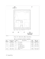
Страница 254: ...Figure 12 1 Top View Major Assemblies 12 4 Replaceable Parts ...
Страница 290: ...Figure 12 36 Main Frame Assembly Parts 17 19 12 40 Replaceable Parts ...
Страница 294: ......
Страница 302: ...Figure B 1 Connector Locations On the A20 Motherboard Circuit Side B 2 A20 Motherboard Pin Assignment ...
Страница 303: ...Figure B 2 Pin Assignment On the A20 Motherboard Circuit Side A20 Motherboard Pin Assignment B 3 ...
Страница 308: ......
Страница 311: ...Figure C 1 Power Cable Supplied Power Requirement C 3 ...
Страница 312: ......
Страница 324: ......


