


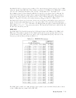


T
able
11-2.
RF
OUT
P
ower
,
A3A3
Output,
and
A7
Attenuator
(Non-P
ower
Sweep)
RF
OUT
P
ower
A3A3
Output
A7
Attenuation
0
dBm
<
Setting
+20
dBm
0
dBm
<
Setting
+20
dBm
0
dB
010
dBm
<
P
ower
0
dBm
0
dBm
<
Setting
+20
dBm
10
dB
020
dBm
<
P
ower
010
dBm
0
dBm
<
Setting
+10
dBm
20
dB
030
dBm
<
P
ower
020
dBm
0
dBm
<
Setting
+10
dBm
30
dB
040
dBm
<
P
ower
030
dBm
0
dBm
<
Setting
+10
dBm
40
dB
050
dBm
<
P
ower
040
dBm
0
dBm
<
Setting
+10
dBm
50
dB
060
dBm
P
ower
050
dBm
0
dBm
Setting
+10
dBm
60
dB
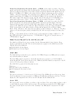
When
making
a
power
sweep
measurement,
the
A7
output
attenuator
cannot
be
changed
during
a
power
sweep
.
Therefore
,
the
applicable
power
sweep
range
is
the
maximum
30
dB
that
is
the
A3A3's
RF
signal
power
range
.
The
A7
setting
is
determined
by
the
stop
power
setting
in
the
power
sweep
measurement.
Also
,
the
allowable
start
power
depends
on
the
stop
power
setting.
T
able
11-3
shows
the
relationship
among
the
stop
power
setting,
the
A7
setting,
and
the
allowable
start
power
in
the
power
sweep
measurement.
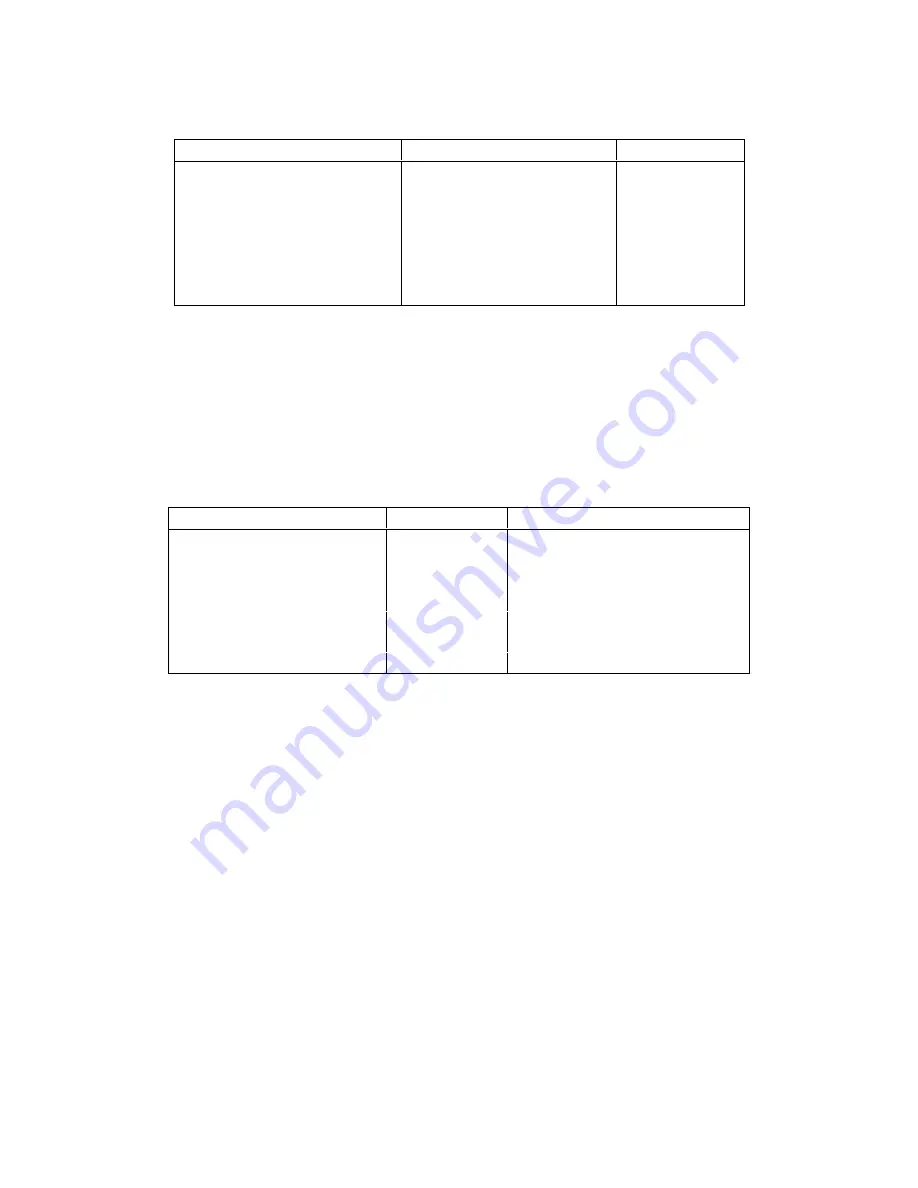
T
able
11-3.
Stop
P
ower
,
A7
Attenuation,
and
Allowable
Start
P
ower
(P
ower
Sweep)
Stop
P
ower
A7
Attenuator
Allowable
Start
P
ower
+10
dB
<
P
ower
+20
dBm
0
dB
010
dBm
P
ower
<
Stop
P
ower
0
dB
<
P
ower
+10
dBm
10
dB
020
dBm
P
ower
<
Stop
P
ower
010
dB
<
P
ower
0
dBm
20
dB
030
dBm
P
ower
<
Stop
P
ower
020
dB
<
P
ower
010
dBm
30
dB
040
dBm
P
ower
<
Stop
P
ower
030
dB
<
P
ower
020
dBm
40
dB
050
dBm
P
ower
<
Stop
P
ower
040
dB
<
P
ower
030
dBm
50
dB
060
dBm
P
ower
<
Stop
P
ower
060
dB
<
P
ower
040
dBm
60
dB
060
dBm
P
ower
<
Stop
P
ower
11-22
Theory
of
Operation
Содержание Agilent 4396B
Страница 10: ......
Страница 32: ......
Страница 39: ...Figure 2 3 40 MHz Reference Oscillator Frequency Adjustment Location Adjustments and Correction Constants 2 7 ...
Страница 43: ...Figure 2 7 CAL OUT Level Adjustment Location Adjustments and Correction Constants 2 11 ...
Страница 46: ...Figure 2 10 Comb Generator Output 2 14 Adjustments and Correction Constants ...
Страница 54: ...Figure 2 18 Plug Locations 19 Replace the A6 board into the slot 2 22 Adjustments and Correction Constants ...
Страница 62: ...Figure 2 26 Final Gain Adjustment Location 2 30 Adjustments and Correction Constants ...
Страница 70: ...Figure 2 34 IF Gain Errors Correction Constants Setup 2 2 38 Adjustments and Correction Constants ...
Страница 76: ...Figure 3 1 Troubleshooting Organization 3 2 T roubleshooting ...
Страница 84: ......
Страница 90: ...Figure 5 1 Power Supply Lines Simpli ed Block Diagram 5 2 Power Supply T roubleshooting ...
Страница 107: ...Figure 5 12 Power Supply Block Diagram 1 Power Supply T roubleshooting 5 19 ...
Страница 108: ...Figure 5 13 Power Supply Block Diagram 2 5 20 Power Supply T roubleshooting ...
Страница 109: ...Figure 5 14 Power Supply Block Diagram 3 Power Supply T roubleshooting 5 21 ...
Страница 110: ......
Страница 112: ...Figure 6 1 Digital Control Group Simpli ed Block Diagram 6 2 Digital Control T roubleshooting ...
Страница 124: ......
Страница 126: ...Figure 7 1 Source Group Block Diagram 7 2 Source Group T roubleshooting ...
Страница 160: ...Figure 8 1 Receiver Group Simpli ed Block Diagram 8 2 Receiver Group T roubleshooting ...
Страница 168: ......
Страница 184: ...Figure 10 6 External Test Setup 1 Figure 10 7 External Test Setup 2 10 10 Service Key Menus ...
Страница 185: ...Figure 10 8 External Test Setup 3 Figure 10 9 External Test Setup 4 Service Key Menus 10 11 ...
Страница 226: ...Figure 11 3 Power Supply Functional Group Simpli ed Block Diagram 11 6 Theory of Operation ...
Страница 231: ...Figure 11 5 Digital Control Group Simpli ed Block Diagram Theory of Operation 11 11 ...
Страница 235: ...Figure 11 6 Source Simpli ed Block Diagram Theory of Operation 11 15 ...
Страница 244: ...Figure 11 7 Receiver Simpli ed Block Diagram 11 24 Theory of Operation ...
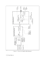
Страница 249: ...Figure IDC5S11001 here Figure 11 8 4396B Source Group Block Diagram Theory of Operation 11 29 ...
Страница 250: ...Figure IDC5S11002 here Figure 11 9 4396B Receiver Group Block Diagram 11 30 Theory of Operation ...
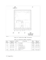
Страница 254: ...Figure 12 1 Top View Major Assemblies 12 4 Replaceable Parts ...
Страница 290: ...Figure 12 36 Main Frame Assembly Parts 17 19 12 40 Replaceable Parts ...
Страница 294: ......
Страница 302: ...Figure B 1 Connector Locations On the A20 Motherboard Circuit Side B 2 A20 Motherboard Pin Assignment ...
Страница 303: ...Figure B 2 Pin Assignment On the A20 Motherboard Circuit Side A20 Motherboard Pin Assignment B 3 ...
Страница 308: ......
Страница 311: ...Figure C 1 Power Cable Supplied Power Requirement C 3 ...
Страница 312: ......
Страница 324: ......


