

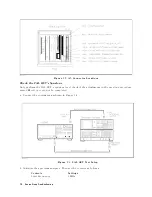


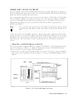


b.
Press
4
Meas
5 ,
NNNNNNNNNNNNNNNNNNNNNNNNNNNNNNNNNNNNNNNNN
ANALYZER
TYPE
,
NNNNNNNNNNNNNNNNNNNNNNNNNNNNNNNNNNNNNNNNNNNNNNNNNNNNN
SPECTRUM
ANALYZER
,
4
Preset
5 ,
4
Sw
eep
5 ,
NNNNNNNNNNNNNNNNNNNNNNNNNNNNNNNN
SWEEP
TIME
,
4
2
5 ,
4
0
5 ,
4
x1
5 .
During
this
procedure
,
the
start
and
stop
frequencies
are
set
to
0
MHz
and
1.8
GHz,
respectively
.
These
start
and
stop
settings
set
the
1st
LO
OSC
to
the
single-loop
mode
and
sweep
the
frequency
from
2.05858
GHz
(at
the
start
frequency
0
Hz)
to
3.85858
GHz
(at
the
stop
frequency
1.8
GHz).
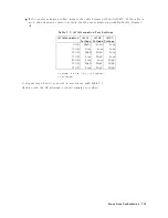
c.
Initialize
the
spectrum
analyzer
.
Then
set
the
controls
as
follows:
(The
sweep
time
must
be
less
than
24
msec
.)
Controls
Settings
Start
Frequency
2
GHz
Stop
Frequency
4
GHz
Reference
Level
10
dBm
Max
Hold
ON
d.
On
the
4396B
,
press
4
T
rigger
5 ,
NNNNNNNNNNNNNNNNNNNNNNNNNNNNNNNNNNNNNNNNNNNNNNN
MEASURE
RESTART
.
W
ait
for
the
completion
of
the
sweep
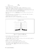
e.
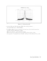
Check
that
the
signal
level
is
05
dBm
to
+5
dBm
over
the
frequency
range
of
2.058
G
MHz
to
3.858
GHz.
The
displayed
trace
should
be
as
shown
in
Figure
7-17 .
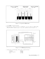
The
measured
level
is
lower
than
the
actual
level
due
to
the
BNC(m)-BNC(m)
cable's
insertion
loss
at
high
frequencies
.
If
the
measured
level
is
lower
than
the
limit,
measure
the
cable's
loss
and
compensate
the
signal
level
by
the
cable's
loss
.
If
the
signal
level
and
the
trace
are
good,
continue
with
the
next
step
.
If
the
signal
level
or
the
trace
is
bad,
the
A4A1
1st
LO
is
faulty
.
Replace
A4.
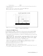
Figure
7-17.
Typical
1st
LO
OSC
Signal
(Single
Mode)
at
A4A1J3
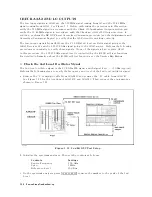
f.
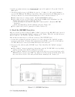
On
the
4396B
,
press
4
Span
5 ,
4
4
5 ,
4
5
5 ,
4
M/
5 .
During
this
procedure
,
the
start
and
stop
frequencies
are
set
to
877.5
MHz
and
922.5
MHz,
respectively
.
These
start
and
stop
settings
set
the
1st
LO
OSC
to
the
triple-loop
mode
and
sweep
the
1st
LO
OSC
frequency
from
2.93608
GHz
(at
the
start
frequency
877.5
MHz)
to
2.98108
GHz
(at
the
stop
frequency
922.5
GHz).
7-20
Source
Group
T
roubleshooting
Содержание Agilent 4396B
Страница 10: ......
Страница 32: ......
Страница 39: ...Figure 2 3 40 MHz Reference Oscillator Frequency Adjustment Location Adjustments and Correction Constants 2 7 ...
Страница 43: ...Figure 2 7 CAL OUT Level Adjustment Location Adjustments and Correction Constants 2 11 ...
Страница 46: ...Figure 2 10 Comb Generator Output 2 14 Adjustments and Correction Constants ...
Страница 54: ...Figure 2 18 Plug Locations 19 Replace the A6 board into the slot 2 22 Adjustments and Correction Constants ...
Страница 62: ...Figure 2 26 Final Gain Adjustment Location 2 30 Adjustments and Correction Constants ...
Страница 70: ...Figure 2 34 IF Gain Errors Correction Constants Setup 2 2 38 Adjustments and Correction Constants ...
Страница 76: ...Figure 3 1 Troubleshooting Organization 3 2 T roubleshooting ...
Страница 84: ......
Страница 90: ...Figure 5 1 Power Supply Lines Simpli ed Block Diagram 5 2 Power Supply T roubleshooting ...
Страница 107: ...Figure 5 12 Power Supply Block Diagram 1 Power Supply T roubleshooting 5 19 ...
Страница 108: ...Figure 5 13 Power Supply Block Diagram 2 5 20 Power Supply T roubleshooting ...
Страница 109: ...Figure 5 14 Power Supply Block Diagram 3 Power Supply T roubleshooting 5 21 ...
Страница 110: ......
Страница 112: ...Figure 6 1 Digital Control Group Simpli ed Block Diagram 6 2 Digital Control T roubleshooting ...
Страница 124: ......
Страница 126: ...Figure 7 1 Source Group Block Diagram 7 2 Source Group T roubleshooting ...
Страница 160: ...Figure 8 1 Receiver Group Simpli ed Block Diagram 8 2 Receiver Group T roubleshooting ...
Страница 168: ......
Страница 184: ...Figure 10 6 External Test Setup 1 Figure 10 7 External Test Setup 2 10 10 Service Key Menus ...
Страница 185: ...Figure 10 8 External Test Setup 3 Figure 10 9 External Test Setup 4 Service Key Menus 10 11 ...
Страница 226: ...Figure 11 3 Power Supply Functional Group Simpli ed Block Diagram 11 6 Theory of Operation ...
Страница 231: ...Figure 11 5 Digital Control Group Simpli ed Block Diagram Theory of Operation 11 11 ...
Страница 235: ...Figure 11 6 Source Simpli ed Block Diagram Theory of Operation 11 15 ...
Страница 244: ...Figure 11 7 Receiver Simpli ed Block Diagram 11 24 Theory of Operation ...
Страница 249: ...Figure IDC5S11001 here Figure 11 8 4396B Source Group Block Diagram Theory of Operation 11 29 ...
Страница 250: ...Figure IDC5S11002 here Figure 11 9 4396B Receiver Group Block Diagram 11 30 Theory of Operation ...
Страница 254: ...Figure 12 1 Top View Major Assemblies 12 4 Replaceable Parts ...
Страница 290: ...Figure 12 36 Main Frame Assembly Parts 17 19 12 40 Replaceable Parts ...
Страница 294: ......
Страница 302: ...Figure B 1 Connector Locations On the A20 Motherboard Circuit Side B 2 A20 Motherboard Pin Assignment ...
Страница 303: ...Figure B 2 Pin Assignment On the A20 Motherboard Circuit Side A20 Motherboard Pin Assignment B 3 ...
Страница 308: ......
Страница 311: ...Figure C 1 Power Cable Supplied Power Requirement C 3 ...
Страница 312: ......
Страница 324: ......


