


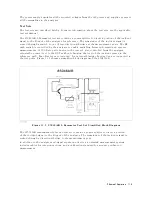


ANAL
YZER
FUNCTIONAL
GROUPS
The
analyzer
consists
of
four
main
functional
groups:
a
source
,
a
receiver
,
a
digital
control,
and
a
power
supply
.
Each
group
consists
of
several
major
assemblies
,
and
performs
a
distinct
function
in
the
analyzer
.
However
,
all
the
groups
are
interrelated
to
some
extent
and
aect
each
other's
performance
.
P
ower
Supply:
The
power
supply
functional
group
consists
of
the
A40
preregulator
,
the
A50
DC-DC
converter
and
the
A2
post-regulator
.
It
supplies
power
to
the
other
assemblies
in
the
analyzer
.
Digital
Control:
The
digital
control
group
consists
of
the
A1
CPU
,
the
A30
keyboard,
the
A31
I/O
connector
,
the
A32
Instrument
B
ASIC
interface
,
the
A51
GSP
(Graphics
System
Processor),
the
A52
LCD
(Liquid
Crystal
Display),
and
the
A53
FDD
(Flexible
Disk
Drive).
These
assemblies
combine
to
provide
digital
control
for
the
analyzer
and
an
S-P
arameter
T
est
set
(if
used).
Source:
The
source
group
consists
of
the
A5
synthesizer
,
the
A4A1
1st
LO
(1st
local
oscillator),
the
A3A1
ALC
(automatic
leveling
control),
the
A3A2
2nd
LO
(second
local
oscillator),
the
A3A3
source
,
the
A7
output
attenuator
,
and
the
A60
high
stability
frequency
reference
(option
1D5
only).
The
source
supplies
a
phase-locked
RF
signal
to
the
device
under
test
and
supplies
the
1st
and
2nd
local
oscillator
signals
to
the
receiver
.
Receiver:
The
receiver
group
consists
of
the
A9
input
multiplexer
,
the
A8
input
attenuator
,
A4A2
receiver
RF
,
and
the
A6
receiver
IF
.
The
receiver
measures
and
processes
RF
signal
inputs
for
display
.
The
following
pages
describe
the
operation
of
the
functional
groups
.
11-4
Theory
of
Operation
Содержание Agilent 4396B
Страница 10: ......
Страница 32: ......
Страница 39: ...Figure 2 3 40 MHz Reference Oscillator Frequency Adjustment Location Adjustments and Correction Constants 2 7 ...
Страница 43: ...Figure 2 7 CAL OUT Level Adjustment Location Adjustments and Correction Constants 2 11 ...
Страница 46: ...Figure 2 10 Comb Generator Output 2 14 Adjustments and Correction Constants ...
Страница 54: ...Figure 2 18 Plug Locations 19 Replace the A6 board into the slot 2 22 Adjustments and Correction Constants ...
Страница 62: ...Figure 2 26 Final Gain Adjustment Location 2 30 Adjustments and Correction Constants ...
Страница 70: ...Figure 2 34 IF Gain Errors Correction Constants Setup 2 2 38 Adjustments and Correction Constants ...
Страница 76: ...Figure 3 1 Troubleshooting Organization 3 2 T roubleshooting ...
Страница 84: ......
Страница 90: ...Figure 5 1 Power Supply Lines Simpli ed Block Diagram 5 2 Power Supply T roubleshooting ...
Страница 107: ...Figure 5 12 Power Supply Block Diagram 1 Power Supply T roubleshooting 5 19 ...
Страница 108: ...Figure 5 13 Power Supply Block Diagram 2 5 20 Power Supply T roubleshooting ...
Страница 109: ...Figure 5 14 Power Supply Block Diagram 3 Power Supply T roubleshooting 5 21 ...
Страница 110: ......
Страница 112: ...Figure 6 1 Digital Control Group Simpli ed Block Diagram 6 2 Digital Control T roubleshooting ...
Страница 124: ......
Страница 126: ...Figure 7 1 Source Group Block Diagram 7 2 Source Group T roubleshooting ...
Страница 160: ...Figure 8 1 Receiver Group Simpli ed Block Diagram 8 2 Receiver Group T roubleshooting ...
Страница 168: ......
Страница 184: ...Figure 10 6 External Test Setup 1 Figure 10 7 External Test Setup 2 10 10 Service Key Menus ...
Страница 185: ...Figure 10 8 External Test Setup 3 Figure 10 9 External Test Setup 4 Service Key Menus 10 11 ...
Страница 226: ...Figure 11 3 Power Supply Functional Group Simpli ed Block Diagram 11 6 Theory of Operation ...
Страница 231: ...Figure 11 5 Digital Control Group Simpli ed Block Diagram Theory of Operation 11 11 ...
Страница 235: ...Figure 11 6 Source Simpli ed Block Diagram Theory of Operation 11 15 ...
Страница 244: ...Figure 11 7 Receiver Simpli ed Block Diagram 11 24 Theory of Operation ...
Страница 249: ...Figure IDC5S11001 here Figure 11 8 4396B Source Group Block Diagram Theory of Operation 11 29 ...
Страница 250: ...Figure IDC5S11002 here Figure 11 9 4396B Receiver Group Block Diagram 11 30 Theory of Operation ...
Страница 254: ...Figure 12 1 Top View Major Assemblies 12 4 Replaceable Parts ...
Страница 290: ...Figure 12 36 Main Frame Assembly Parts 17 19 12 40 Replaceable Parts ...
Страница 294: ......
Страница 302: ...Figure B 1 Connector Locations On the A20 Motherboard Circuit Side B 2 A20 Motherboard Pin Assignment ...
Страница 303: ...Figure B 2 Pin Assignment On the A20 Motherboard Circuit Side A20 Motherboard Pin Assignment B 3 ...
Страница 308: ......
Страница 311: ...Figure C 1 Power Cable Supplied Power Requirement C 3 ...
Страница 312: ......
Страница 324: ......


