


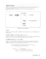


8:
A5
STEP
OSC
Runs
only
when
selected.
It
veries
the
step
oscillator
in
the
A5
synthesizer
.
This
test
sets
the
oscillator
frequency
to
several
frequencies
over
the
entire
range
.
F
or
each
frequency
,
the
test
measures
the
V
CO
tuning
voltage
at
DC
bus
node
19
and
the
frequency
at
frequency
bus
node
3.
It
then
checks
that
each
measured
value
is
within
limits
.
9:
A4A1
1ST
LO
OSC
V
eries
the
1st
LO
oscillator
in
the
A4A1
1st
LO
.
This
test
sets
the
oscillator
frequency
to
several
frequencies
over
the
entire
range
.
F
or
each
frequency
,
the
test
measures
the
V
CO
tuning
voltage
at
DC
bus
node
18
and
checks
that
each
measured
value
is
within
limits
.
10:
A3A2
2ND
LO
OSC
V
eries
the
2nd
LO
oscillator
in
the
A3A2
2nd
LO
.
This
test
measures
the
V
CO
tuning
voltage
at
DC
bus
node
14
and
checks
that
the
measured
value
is
within
limits
.
11:
A3A1
DIVIDER
V
eries
the
divider
circuit
in
the
A3A1
ALC.
This
test
measures
the
frequency
(40
kHz)
at
frequency
bus
node
2
and
checks
that
the
measured
value
is
within
limits
.
12:
A6
3RD
LO
OSC
V
eries
the
3rd
LO
oscillator
on
the
A6
receiver
IF
.
This
test
measures
the
V
CO
tuning
voltage
at
DC
bus
node
23
and
the
frequency
(40
kHz)
at
frequency
bus
node
6.
It
then
checks
that
each
measured
value
is
within
limits
.
13:
A3A1
SOURCE
OSC
V
eries
the
source
oscillator
in
the
A3A1
ALC.
This
test
measures
the
V
CO
tuning
voltage
at
DC
bus
node
13
and
the
frequency
(40
kHz)
at
frequency
bus
node
1.
It
then
checks
that
each
measured
value
is
within
limits
.
14:
A6
3RD
IF
DC
OFFSET
This
test
measures
the
DC
oset
voltages
on
the
0
and
90
paths
in
the
A6
receiver
IF
and
checks
that
each
measured
value
is
within
limits
.
15:
A6
SEQUENCER
V
eries
the
A/D
sequencer
circuit
in
the
A6
receiver
IF
.
This
test
measures
the
frequency
(80
kHz)
of
the
A/D
sequence
output
at
frequency
bus
node
7
and
checks
that
the
measured
value
is
within
limits
.
16:
A3A1
ALC
V
eries
the
ALC
(automatic
leveling
control)
circuit
in
the
A3A1
ALC.
This
test
varies
the
power
level
and
frequency
of
the
RF
OUT
signal.
F
or
each
setting,
the
test
measures
the
voltage
at
DC
bus
nodes
15
and
17
and
checks
that
each
measured
value
is
within
limits
.
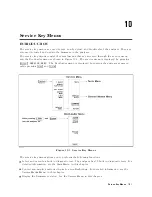
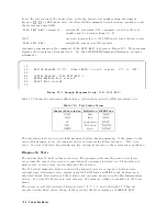
N
NNNNNNNNNNNNNNNNNNNNNNNNNNNNNNNNNNNNNNNNNNNNNNN
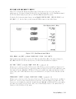
EXTERNAL
TESTS
This
group
of
tests
require
either
external
equipment
and
connections
or
operator
interaction
to
run.
These
tests
are
used
in
the
Troubleshooting
chapter
.
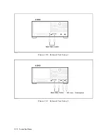
There
are
ve
test
setups
(1
through
5)
for
the
external
tests
as
shown
in
Figure
10-6
through
Figure
10-10.
If
required,
the
external
test
description
indicates
the
test
setup
used
in
that
external
test.
Service
K
ey
Menus
10-9
Содержание Agilent 4396B
Страница 10: ......
Страница 32: ......
Страница 39: ...Figure 2 3 40 MHz Reference Oscillator Frequency Adjustment Location Adjustments and Correction Constants 2 7 ...
Страница 43: ...Figure 2 7 CAL OUT Level Adjustment Location Adjustments and Correction Constants 2 11 ...
Страница 46: ...Figure 2 10 Comb Generator Output 2 14 Adjustments and Correction Constants ...
Страница 54: ...Figure 2 18 Plug Locations 19 Replace the A6 board into the slot 2 22 Adjustments and Correction Constants ...
Страница 62: ...Figure 2 26 Final Gain Adjustment Location 2 30 Adjustments and Correction Constants ...
Страница 70: ...Figure 2 34 IF Gain Errors Correction Constants Setup 2 2 38 Adjustments and Correction Constants ...
Страница 76: ...Figure 3 1 Troubleshooting Organization 3 2 T roubleshooting ...
Страница 84: ......
Страница 90: ...Figure 5 1 Power Supply Lines Simpli ed Block Diagram 5 2 Power Supply T roubleshooting ...
Страница 107: ...Figure 5 12 Power Supply Block Diagram 1 Power Supply T roubleshooting 5 19 ...
Страница 108: ...Figure 5 13 Power Supply Block Diagram 2 5 20 Power Supply T roubleshooting ...
Страница 109: ...Figure 5 14 Power Supply Block Diagram 3 Power Supply T roubleshooting 5 21 ...
Страница 110: ......
Страница 112: ...Figure 6 1 Digital Control Group Simpli ed Block Diagram 6 2 Digital Control T roubleshooting ...
Страница 124: ......
Страница 126: ...Figure 7 1 Source Group Block Diagram 7 2 Source Group T roubleshooting ...
Страница 160: ...Figure 8 1 Receiver Group Simpli ed Block Diagram 8 2 Receiver Group T roubleshooting ...
Страница 168: ......
Страница 184: ...Figure 10 6 External Test Setup 1 Figure 10 7 External Test Setup 2 10 10 Service Key Menus ...
Страница 185: ...Figure 10 8 External Test Setup 3 Figure 10 9 External Test Setup 4 Service Key Menus 10 11 ...
Страница 226: ...Figure 11 3 Power Supply Functional Group Simpli ed Block Diagram 11 6 Theory of Operation ...
Страница 231: ...Figure 11 5 Digital Control Group Simpli ed Block Diagram Theory of Operation 11 11 ...
Страница 235: ...Figure 11 6 Source Simpli ed Block Diagram Theory of Operation 11 15 ...
Страница 244: ...Figure 11 7 Receiver Simpli ed Block Diagram 11 24 Theory of Operation ...
Страница 249: ...Figure IDC5S11001 here Figure 11 8 4396B Source Group Block Diagram Theory of Operation 11 29 ...
Страница 250: ...Figure IDC5S11002 here Figure 11 9 4396B Receiver Group Block Diagram 11 30 Theory of Operation ...
Страница 254: ...Figure 12 1 Top View Major Assemblies 12 4 Replaceable Parts ...
Страница 290: ...Figure 12 36 Main Frame Assembly Parts 17 19 12 40 Replaceable Parts ...
Страница 294: ......
Страница 302: ...Figure B 1 Connector Locations On the A20 Motherboard Circuit Side B 2 A20 Motherboard Pin Assignment ...
Страница 303: ...Figure B 2 Pin Assignment On the A20 Motherboard Circuit Side A20 Motherboard Pin Assignment B 3 ...
Страница 308: ......
Страница 311: ...Figure C 1 Power Cable Supplied Power Requirement C 3 ...
Страница 312: ......
Страница 324: ......


