


The
power
supply
regulates
all
the
required
voltages
from
the
A
C
power
and
supplies
power
to
all
the
assemblies
in
the
analyzer
.
T
est
Sets
The
test
sets
are
described
briey
.
F
or
more
information
about
the
test
sets
,
see
the
applicable
test
set
manual.
The
85046A/B
S-P
arameter
test
set
contains
a
power
splitter
to
divert
a
portion
of
the
incident
signal
to
the
R
input
of
the
analyzer
for
reference
.
The
remainder
of
the
incident
signal
is
routed
through
a
switch
to
one
of
two
directional
bridges
at
the
measurement
ports
.
The
RF
path
switch
is
controlled
by
the
analyzer
to
enable
switching
between
forward
and
reverse
measurements
.
A
70
dB
step
attenuator
in
the
test
set,
also
controlled
from
the
analyzer
,
adjusts
the
power
level
to
the
DUT
without
changing
the
level
of
the
incident
power
in
the
reference
path.
Two
bias
tees
are
included,
for
external
biasing
of
active
devices
connected
to
the
test
ports
.
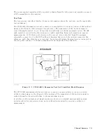
Figure
11-2
shows
a
simplied
block
diagram
of
the
85046A/B
.
Figure
11-2.
85046A/B
S-P
arameter
T
est
Set
Simplied
Block
Diagram
The
87512A/B
transmission/reection
test
set
contains
a
power
splitter
to
divert
a
portion
of
the
incident
signal
to
the
R
input
of
the
analyzer
.
The
remainder
of
the
incident
signal
is
routed
through
a
directional
bridge
to
the
measurement
port.
In
addition
to
the
analyzer
and
signal
separation
devices
,
a
network
measurement
system
includes
cables
for
interconnections
,
and
a
calibration
standard
for
accuracy
enhanced
measurement.
Theory
of
Operation
11-3
Содержание Agilent 4396B
Страница 10: ......
Страница 32: ......
Страница 39: ...Figure 2 3 40 MHz Reference Oscillator Frequency Adjustment Location Adjustments and Correction Constants 2 7 ...
Страница 43: ...Figure 2 7 CAL OUT Level Adjustment Location Adjustments and Correction Constants 2 11 ...
Страница 46: ...Figure 2 10 Comb Generator Output 2 14 Adjustments and Correction Constants ...
Страница 54: ...Figure 2 18 Plug Locations 19 Replace the A6 board into the slot 2 22 Adjustments and Correction Constants ...
Страница 62: ...Figure 2 26 Final Gain Adjustment Location 2 30 Adjustments and Correction Constants ...
Страница 70: ...Figure 2 34 IF Gain Errors Correction Constants Setup 2 2 38 Adjustments and Correction Constants ...
Страница 76: ...Figure 3 1 Troubleshooting Organization 3 2 T roubleshooting ...
Страница 84: ......
Страница 90: ...Figure 5 1 Power Supply Lines Simpli ed Block Diagram 5 2 Power Supply T roubleshooting ...
Страница 107: ...Figure 5 12 Power Supply Block Diagram 1 Power Supply T roubleshooting 5 19 ...
Страница 108: ...Figure 5 13 Power Supply Block Diagram 2 5 20 Power Supply T roubleshooting ...
Страница 109: ...Figure 5 14 Power Supply Block Diagram 3 Power Supply T roubleshooting 5 21 ...
Страница 110: ......
Страница 112: ...Figure 6 1 Digital Control Group Simpli ed Block Diagram 6 2 Digital Control T roubleshooting ...
Страница 124: ......
Страница 126: ...Figure 7 1 Source Group Block Diagram 7 2 Source Group T roubleshooting ...
Страница 160: ...Figure 8 1 Receiver Group Simpli ed Block Diagram 8 2 Receiver Group T roubleshooting ...
Страница 168: ......
Страница 184: ...Figure 10 6 External Test Setup 1 Figure 10 7 External Test Setup 2 10 10 Service Key Menus ...
Страница 185: ...Figure 10 8 External Test Setup 3 Figure 10 9 External Test Setup 4 Service Key Menus 10 11 ...
Страница 226: ...Figure 11 3 Power Supply Functional Group Simpli ed Block Diagram 11 6 Theory of Operation ...
Страница 231: ...Figure 11 5 Digital Control Group Simpli ed Block Diagram Theory of Operation 11 11 ...
Страница 235: ...Figure 11 6 Source Simpli ed Block Diagram Theory of Operation 11 15 ...
Страница 244: ...Figure 11 7 Receiver Simpli ed Block Diagram 11 24 Theory of Operation ...
Страница 249: ...Figure IDC5S11001 here Figure 11 8 4396B Source Group Block Diagram Theory of Operation 11 29 ...
Страница 250: ...Figure IDC5S11002 here Figure 11 9 4396B Receiver Group Block Diagram 11 30 Theory of Operation ...
Страница 254: ...Figure 12 1 Top View Major Assemblies 12 4 Replaceable Parts ...
Страница 290: ...Figure 12 36 Main Frame Assembly Parts 17 19 12 40 Replaceable Parts ...
Страница 294: ......
Страница 302: ...Figure B 1 Connector Locations On the A20 Motherboard Circuit Side B 2 A20 Motherboard Pin Assignment ...
Страница 303: ...Figure B 2 Pin Assignment On the A20 Motherboard Circuit Side A20 Motherboard Pin Assignment B 3 ...
Страница 308: ......
Страница 311: ...Figure C 1 Power Cable Supplied Power Requirement C 3 ...
Страница 312: ......
Страница 324: ......


