


The
receiver
has
four
inputs
(R,
A,
B
,
and
S).
The
receiver
is
used
in
both
the
network
analyzer
mode
and
the
spectrum
analyzer
mode
.
T
o
operate
in
both
the
network
and
spectrum
analyzer
modes
using
one
receiver
,
the
receiver
has
two
switches
,
an
Input
Multiplexer
and
a
NA/SA
switch
at
the
front
end.
One
of
the
signals
from
the
four
inputs
(R,
A,
B
,
or
S)
is
switched
to
the
circuit
following
these
switches
.
Spectrum
Analyzer
Operation
A
spectrum
analyzer
measures
the
amplitude
and
frequency
of
a
signal
spectral
line
by
sweeping
the
tuning
frequency
of
the
receiver
.
A
typical
spectrum
analyzer
consists
of
four
main
groups:
a
synthesizer
,
a
receiver
,
a
digital
control,
and
a
power
supply
.
In
the
4396B
,
the
synthesizer
is
included
in
the
source
.
The
RF
signal
to
be
tested
is
applied
to
the
receiver
.
The
receiver
converts
the
signal
frequency
to
a
20
kHz
or
DC
3rd
IF
(third
intermediate
frequency)
for
signal
processing.
It
then
converts
the
signal
to
a
digital
value
using
the
A/D
(analog
to
digital)
converter
.
The
digitized
raw
data
is
then
transferred
to
the
digital
control
group
.
The
raw
data
is
processed
in
the
digital
control
group
.
The
formatted
data
is
nally
routed
to
the
LCD
for
display
,
and
to
the
GPIB
for
remote
operation.
F
or
details
of
the
data
processing
signal
ow
,
see
the
Analyzer
F
eature
chapter
of
the
4396B
Function
R
eference
Manual.
In
the
4396B
,
the
receiver
requires
three
local
oscillator
signals
to
convert
the
RF
signal
to
the
1st/2nd/3rd
IF
signals
.
The
synthesizer
in
the
analyzer's
source
generates
the
1st
and
2nd
local
oscillator
signals
and
supplies
these
signals
to
the
receiver
.
The
third
local
oscillator
signal
is
generated
in
the
receiver
.
The
power
supply
regulates
all
the
required
voltages
from
the
A
C
power
and
supplies
power
to
all
the
assemblies
in
the
analyzer
.
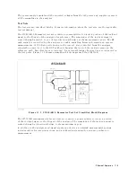
Network
Analyzer
Operation
A
network
analyzer
measures
the
reection
and
transmission
characteristics
of
devices
by
applying
a
known
swept
signal
and
measuring
the
response
of
the
DUT
(device
under
test).
A
typical
network
analyzer
system
consists
of
a
network
analyzer
and
signal
separation
devices
(a
test
set
or
power
splitter).
Furthermore
,
the
network
analyzer
consists
of
four
main
groups:
a
source
,
a
receiver
,
a
digital
control,
and
a
power
supply
.
The
4396B's
built-in
synthesized
source
generates
a
known
CW
(continuous
wave)
or
swept
RF
signal
in
the
range
of
100
kHz
to
1.8
GHz.
The
RF
signal
power
is
leveled
using
the
ALC
(automatic
leveling
control),
to
a
maximum
level
of
+20
dBm.
In
addition,
the
source
supplies
the
local
oscillator
signals
to
the
receiver
.
The
source's
RF
signal
is
applied
to
the
DUT
through
the
signal
separation
device
.
The
signal
transmitted
through
the
device
or
reected
from
its
input
goes
to
the
B
and/or
A
inputs
of
the
receiver
and
is
compared
with
the
incident
signal
at
the
R
input.
The
signal
separation
device
in
the
network
analyzer
system
is
an
85046A/B
S-P
arameter
test
set,
an
87512A/B
transmission/reection
test
set,
or
an
11850C/D
or
11667A
power
splitter
.
The
test
sets
are
described
below
.
The
receiver
converts
the
RF
input
frequency
to
a
20
kHz
or
DC
3rd
IF
for
signal
processing.
It
then
converts
the
signal
to
a
digital
signal
using
the
A/D
converter
.
The
digitized
raw
data
is
transferred
to
the
digital
control
group
.
The
raw
data
is
then
processed
in
the
digital
control.
The
formatted
data
is
nally
routed
to
the
LCD
for
display
,
and
to
the
GPIB
for
remote
operation.
F
or
details
of
the
data
processing
signal
ow
,
see
the
Analyzer
F
eature
chapter
of
the
4396B
Function
R
eference
Manual.
11-2
Theory
of
Operation
Содержание Agilent 4396B
Страница 10: ......
Страница 32: ......
Страница 39: ...Figure 2 3 40 MHz Reference Oscillator Frequency Adjustment Location Adjustments and Correction Constants 2 7 ...
Страница 43: ...Figure 2 7 CAL OUT Level Adjustment Location Adjustments and Correction Constants 2 11 ...
Страница 46: ...Figure 2 10 Comb Generator Output 2 14 Adjustments and Correction Constants ...
Страница 54: ...Figure 2 18 Plug Locations 19 Replace the A6 board into the slot 2 22 Adjustments and Correction Constants ...
Страница 62: ...Figure 2 26 Final Gain Adjustment Location 2 30 Adjustments and Correction Constants ...
Страница 70: ...Figure 2 34 IF Gain Errors Correction Constants Setup 2 2 38 Adjustments and Correction Constants ...
Страница 76: ...Figure 3 1 Troubleshooting Organization 3 2 T roubleshooting ...
Страница 84: ......
Страница 90: ...Figure 5 1 Power Supply Lines Simpli ed Block Diagram 5 2 Power Supply T roubleshooting ...
Страница 107: ...Figure 5 12 Power Supply Block Diagram 1 Power Supply T roubleshooting 5 19 ...
Страница 108: ...Figure 5 13 Power Supply Block Diagram 2 5 20 Power Supply T roubleshooting ...
Страница 109: ...Figure 5 14 Power Supply Block Diagram 3 Power Supply T roubleshooting 5 21 ...
Страница 110: ......
Страница 112: ...Figure 6 1 Digital Control Group Simpli ed Block Diagram 6 2 Digital Control T roubleshooting ...
Страница 124: ......
Страница 126: ...Figure 7 1 Source Group Block Diagram 7 2 Source Group T roubleshooting ...
Страница 160: ...Figure 8 1 Receiver Group Simpli ed Block Diagram 8 2 Receiver Group T roubleshooting ...
Страница 168: ......
Страница 184: ...Figure 10 6 External Test Setup 1 Figure 10 7 External Test Setup 2 10 10 Service Key Menus ...
Страница 185: ...Figure 10 8 External Test Setup 3 Figure 10 9 External Test Setup 4 Service Key Menus 10 11 ...
Страница 226: ...Figure 11 3 Power Supply Functional Group Simpli ed Block Diagram 11 6 Theory of Operation ...
Страница 231: ...Figure 11 5 Digital Control Group Simpli ed Block Diagram Theory of Operation 11 11 ...
Страница 235: ...Figure 11 6 Source Simpli ed Block Diagram Theory of Operation 11 15 ...
Страница 244: ...Figure 11 7 Receiver Simpli ed Block Diagram 11 24 Theory of Operation ...
Страница 249: ...Figure IDC5S11001 here Figure 11 8 4396B Source Group Block Diagram Theory of Operation 11 29 ...
Страница 250: ...Figure IDC5S11002 here Figure 11 9 4396B Receiver Group Block Diagram 11 30 Theory of Operation ...
Страница 254: ...Figure 12 1 Top View Major Assemblies 12 4 Replaceable Parts ...
Страница 290: ...Figure 12 36 Main Frame Assembly Parts 17 19 12 40 Replaceable Parts ...
Страница 294: ......
Страница 302: ...Figure B 1 Connector Locations On the A20 Motherboard Circuit Side B 2 A20 Motherboard Pin Assignment ...
Страница 303: ...Figure B 2 Pin Assignment On the A20 Motherboard Circuit Side A20 Motherboard Pin Assignment B 3 ...
Страница 308: ......
Страница 311: ...Figure C 1 Power Cable Supplied Power Requirement C 3 ...
Страница 312: ......
Страница 324: ......


