


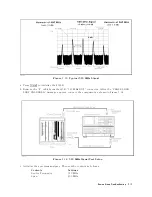


CHECK
A3A2
2ND
LO
OUTPUTS
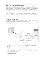
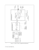
The
two
input
signals
to
A3A2
are
the
520
MHz
signal
coming
from
A5
and
the
21.42
MHz
signal
coming
from
A3A1.
See
Figure
7-1.
Before
performing
the
procedures
in
this
section,
verify
the
520
MHz
signal
in
accordance
with
the
Check
A5
Synthesizer
Outputs
section
and
verify
the
21.42
MHz
signal
in
accordance
with
the
Check
an
A3A1
ALC
Output
section.
In
addition,
perform
the
RF
OUT
Level
Correction
Constants
procedure
(see
the
A
djustments
and
Correction
Constants
chapter)
to
verify
that
the
ALC
circuit
is
working
correctly
.
The
two
output
signals
from
A3A2
are
the
2.08
GHz
2nd
local
oscillator
signal
going
to
the
A4A2
Receiver
IF
and
the
2.05858
GHz
signal
going
to
the
A3A3
source
.
P
erform
the
following
procedures
sequentially
to
verify
these
signals
.
If
one
of
the
signals
is
bad,
replace
A3A2.
In
this
procedure
,
the
2.05858
GHz
signal
level
is
controlled
by
the
4396B
self-test
functions
.
F
or
detailed
information
about
the
4396B
self-test
functions
,
see
the
Service
K
ey
Menus.
1.
Check
the
2nd
Local
Oscillator
Signal
The
2nd
local
oscillator
signal
is
the
2.08
GHz
CW
signal
a
with
signal
level
>
+7
dBm
(typical).
P
erform
the
following
steps
to
verify
the
frequency
and
level
of
the
2nd
local
oscillator
signal:
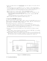
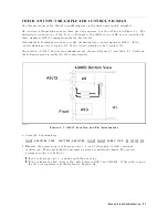
a.
Remove
the
\I"
semi-rigid
cable
from
A3A2J19
and
remove
the
\D"
cable
from
A3A1J3.
See
Figure
7-22
for
the
locations
of
A3A2J19
and
A3A1J3.
Then
connect
the
equipment
as
shown
in
Figure
7-22.
Figure
7-22.
2nd
LO
OSC
T
est
Setup
b.
Initialize
the
spectrum
analyzer
.
Then
set
the
controls
as
follows:
Controls
Settings
Center
Frequency
2.08
GHz
Span
1
MHz
Reference
Level
20
dBm
c.
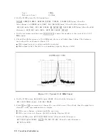
On
the
spectrum
analyzer
,
press
4
PEAK
SEARCH
5
to
move
the
marker
to
the
peak
of
the
2nd
Local.
7-26
Source
Group
T
roubleshooting
Содержание Agilent 4396B
Страница 10: ......
Страница 32: ......
Страница 39: ...Figure 2 3 40 MHz Reference Oscillator Frequency Adjustment Location Adjustments and Correction Constants 2 7 ...
Страница 43: ...Figure 2 7 CAL OUT Level Adjustment Location Adjustments and Correction Constants 2 11 ...
Страница 46: ...Figure 2 10 Comb Generator Output 2 14 Adjustments and Correction Constants ...
Страница 54: ...Figure 2 18 Plug Locations 19 Replace the A6 board into the slot 2 22 Adjustments and Correction Constants ...
Страница 62: ...Figure 2 26 Final Gain Adjustment Location 2 30 Adjustments and Correction Constants ...
Страница 70: ...Figure 2 34 IF Gain Errors Correction Constants Setup 2 2 38 Adjustments and Correction Constants ...
Страница 76: ...Figure 3 1 Troubleshooting Organization 3 2 T roubleshooting ...
Страница 84: ......
Страница 90: ...Figure 5 1 Power Supply Lines Simpli ed Block Diagram 5 2 Power Supply T roubleshooting ...
Страница 107: ...Figure 5 12 Power Supply Block Diagram 1 Power Supply T roubleshooting 5 19 ...
Страница 108: ...Figure 5 13 Power Supply Block Diagram 2 5 20 Power Supply T roubleshooting ...
Страница 109: ...Figure 5 14 Power Supply Block Diagram 3 Power Supply T roubleshooting 5 21 ...
Страница 110: ......
Страница 112: ...Figure 6 1 Digital Control Group Simpli ed Block Diagram 6 2 Digital Control T roubleshooting ...
Страница 124: ......
Страница 126: ...Figure 7 1 Source Group Block Diagram 7 2 Source Group T roubleshooting ...
Страница 160: ...Figure 8 1 Receiver Group Simpli ed Block Diagram 8 2 Receiver Group T roubleshooting ...
Страница 168: ......
Страница 184: ...Figure 10 6 External Test Setup 1 Figure 10 7 External Test Setup 2 10 10 Service Key Menus ...
Страница 185: ...Figure 10 8 External Test Setup 3 Figure 10 9 External Test Setup 4 Service Key Menus 10 11 ...
Страница 226: ...Figure 11 3 Power Supply Functional Group Simpli ed Block Diagram 11 6 Theory of Operation ...
Страница 231: ...Figure 11 5 Digital Control Group Simpli ed Block Diagram Theory of Operation 11 11 ...
Страница 235: ...Figure 11 6 Source Simpli ed Block Diagram Theory of Operation 11 15 ...
Страница 244: ...Figure 11 7 Receiver Simpli ed Block Diagram 11 24 Theory of Operation ...
Страница 249: ...Figure IDC5S11001 here Figure 11 8 4396B Source Group Block Diagram Theory of Operation 11 29 ...
Страница 250: ...Figure IDC5S11002 here Figure 11 9 4396B Receiver Group Block Diagram 11 30 Theory of Operation ...
Страница 254: ...Figure 12 1 Top View Major Assemblies 12 4 Replaceable Parts ...
Страница 290: ...Figure 12 36 Main Frame Assembly Parts 17 19 12 40 Replaceable Parts ...
Страница 294: ......
Страница 302: ...Figure B 1 Connector Locations On the A20 Motherboard Circuit Side B 2 A20 Motherboard Pin Assignment ...
Страница 303: ...Figure B 2 Pin Assignment On the A20 Motherboard Circuit Side A20 Motherboard Pin Assignment B 3 ...
Страница 308: ......
Страница 311: ...Figure C 1 Power Cable Supplied Power Requirement C 3 ...
Страница 312: ......
Страница 324: ......


