TOSHIBA
TMPR3904F Rev. 2.0
189
12.4.12 Parity control
In a transfer operation, the parity control circuit automatically generates a parity by the data that
were written into the transfer shift register; and the parity is stored to the bit7 (the highest-order)
of the transfer shift register when the data length is 7 bits and to the TWUB of the line control
register when the data length is 8 bits to transfer it.
In a receive operation, a parity check is conducted when data have been written from the receive
shift register to the receive read buffer. A comparison is made with the parity bit stored in the
bit7 (the highest-order) of the read buffer when the data length is 7 bits and with the parity bit
stored in the RWUB of the line control register when the data length is 8 bits; and when they do
not match, a parity error occurs.
12.4.13 Error flag
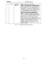
Overrun error
When there are valid data in the receive read buffer, an overrun error occurs if all the bits of the
next data are received by the received shift register. Also when the receive FIFO buffer has
become full, it occurs. A flag is hoisted in the UOER of the line status register. When the ERIE
of the interrupt control register is 1, an error interrupt (SINTREQ*) shall be asserted.
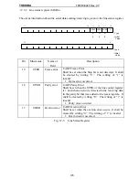
Parity error
When a parity error has occurred, a flag is hoisted in the UPER of the line status register. When
the ERIE of the interrupt control register is 1, an error interrupt (SINTREQ*) shall be asserted.
Framing error
When a 0 is detected in the stop bit of the receive data (majority logic in the sampling at the 7th,
8th, and 9th clocks of the SIOCLK), a framing error occurs. A flag is hoisted in the UFER of
the line status register. When the ERIE of the interrupt control register is 1, an error interrupt
(SINTREQ*) shall be asserted.
12.4.14 Multi-controller system
When the register UMODE is 10 or 11, it is the multi-controller system mode. The multi-
controller system sends data to the selected slave controller after the master controller sends an
address (ID) to a slave controller to select the slave controller. Slave controllers that were not
selected ignore the data. The sending of the address (ID) is conducted by setting the WUB of
the data frame to 1. The data sending is conducted by setting the WUB to 0. The comparison of
the ID’s are conducted by the software. (Comparison between the ID that the slave controller
received and the ID of the slave controller that the software acknowledges.)
Protocol
(1) The master and slave controllers change to the multi-controller system mode by setting the
UMODE of the line control register to 10 or 11.
Summary of Contents for TMPR3904F
Page 1: ...Users Manual 32bit RISC Microprocessor TX39 family TMPR3904F Rev 2 0 Jan 12 1998 ...
Page 2: ......
Page 9: ...Users Manual 01 1 INTRODUCTION 1 1 Overview ...
Page 11: ...Users Manual 03 1 3 Kind of accessing by the TX3904 ...
Page 12: ...Users Manual 04 1 4 Precautions in the TMPR3904F specification Don t set Don t use ...
Page 13: ...Users Manual 05 Do not use ...
Page 14: ...Users Manual 06 ...
Page 15: ...Users Manual 7 2 FEATURES n n n n n n n n n n n n n ...
Page 16: ...Users Manual 8 ...
Page 18: ...Users Manual 10 ...
Page 19: ...Users Manual 11 4 PINS 4 1 Positions of Pins ...
Page 20: ...Users Manual 12 ...
Page 21: ...Users Manual 13 4 2 Functions of Pins ...
Page 22: ...Users Manual 14 ...
Page 23: ...Users Manual 15 ...
Page 24: ...Users Manual 16 ...
Page 26: ...Users Manual 18 5 2 Register Map ...
Page 27: ...Users Manual 19 ...
Page 28: ...Users Manual 20 ...
Page 30: ...Users Manual 22 5 3 2 PIO2 and PIO1 ...
Page 32: ...Users Manual 24 5 3 4 Connection of external bus master 5 3 5 INT 7 0 active status clear ...
Page 33: ...Users Manual 25 5 3 6 INT 7 0 active status set up ...
Page 34: ...Users Manual 26 ...
Page 123: ...TOSHIBA TMPR3904F Rev 2 0 115 26 ...
Page 169: ...TOSHIBA TMPR3904F Rev 2 0 161 26 ...
Page 203: ...TOSHIBA TMPR3904F Rev 2 0 195 ...
Page 230: ......


