TOSHIBA
TMPR3904F Rev. 2.0
97
9.4.3
32/16-bit Static Bus Sizing
The bus width 32/16 bits of the ROM that is connected to the ROM Channel 0 is designated by
an external input pin (BOOT16). The value of this input pin will be taken in to the 16BUS0 of
the channel control register 0 at the time of reset. The bus width of the ROM channel 1 is set up
by the program.
9.4.4
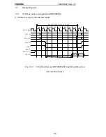
16-bit Bus Access
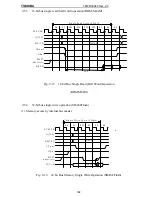
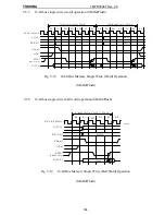
Word/triple-byte access with 16-bit width ROM
If the 16BUSn of the ROM channel control register is 1 when a word/triple-byte access is
requested, the ROMC executes two bus cycles with the timing set up in the register.
Half-word/byte access with 16-bit width ROM
If the 16BUSn of the ROM channel control register is 1 when a 16-bit data access is requested,
the ROMC executes one bus cycle with the timing set up in the register.
9.4.5
Access by External Bus Master
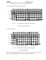
The ROMC drives address(es) with the built-in address counter at the times of page mode access
(page mode mask ROM) and interleave access. When the external bus master conducts a
memory access using the ROMC of the TX3904, an address bus conflict may occur. The
external bus master must stop the drive of the address bus and the BE* at a rising of the
BSTART*. When having received a memory access request from the external bus master, the
ROMC automatically inserts a wait cycle to avoid driving the address, CE*, OE*, and SWE* at
the S1 state. The number of the automatically inserted wait cycles is 1 SYSCLK. AT a single
access, the address output by the external bus master is given to the memory. Therefore, at this
time, please do not stop the address drive.
In the half speed bus mode, please adjust the wait such that the number of the cycles (GCLK) of
the internal system clock should be an even number.
9.4.6
Page mode support
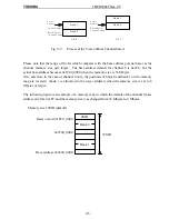
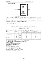
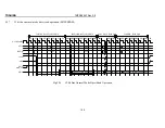
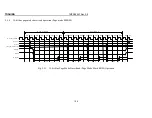
In the case of a page mode mask ROM, the ROM controller conducts page mode access when
the bus master executes the burst mode access. The bus master issues a burst starting address
for the first word, then the ROM controller generates the successive address for the second word
and after. The ROM controller increments address like as 0-4-8-C-10-... if the lower four-bit of
burst starting address is 0x0. On the other hand, it decrements address like as C-8-4-0-... if the
starting address is 0xC.
Summary of Contents for TMPR3904F
Page 1: ...Users Manual 32bit RISC Microprocessor TX39 family TMPR3904F Rev 2 0 Jan 12 1998 ...
Page 2: ......
Page 9: ...Users Manual 01 1 INTRODUCTION 1 1 Overview ...
Page 11: ...Users Manual 03 1 3 Kind of accessing by the TX3904 ...
Page 12: ...Users Manual 04 1 4 Precautions in the TMPR3904F specification Don t set Don t use ...
Page 13: ...Users Manual 05 Do not use ...
Page 14: ...Users Manual 06 ...
Page 15: ...Users Manual 7 2 FEATURES n n n n n n n n n n n n n ...
Page 16: ...Users Manual 8 ...
Page 18: ...Users Manual 10 ...
Page 19: ...Users Manual 11 4 PINS 4 1 Positions of Pins ...
Page 20: ...Users Manual 12 ...
Page 21: ...Users Manual 13 4 2 Functions of Pins ...
Page 22: ...Users Manual 14 ...
Page 23: ...Users Manual 15 ...
Page 24: ...Users Manual 16 ...
Page 26: ...Users Manual 18 5 2 Register Map ...
Page 27: ...Users Manual 19 ...
Page 28: ...Users Manual 20 ...
Page 30: ...Users Manual 22 5 3 2 PIO2 and PIO1 ...
Page 32: ...Users Manual 24 5 3 4 Connection of external bus master 5 3 5 INT 7 0 active status clear ...
Page 33: ...Users Manual 25 5 3 6 INT 7 0 active status set up ...
Page 34: ...Users Manual 26 ...
Page 123: ...TOSHIBA TMPR3904F Rev 2 0 115 26 ...
Page 169: ...TOSHIBA TMPR3904F Rev 2 0 161 26 ...
Page 203: ...TOSHIBA TMPR3904F Rev 2 0 195 ...
Page 230: ......

