TOSHIBA
TMPR3904F Rev. 2.0
187
12.4.5 Receiver Controller
For the receive control, the start bit is detected by the majority logic to start a data receiving
operation. Data receiving is conducted also by the majority logic. The start bit and the
receiving of the data 1 bit are sampled at SIOCLK 16 clocks. The majority logic is implemented
based on the three results of the 7th, 8th, and 9th clocks. (The data that are the same for two or
more of the three results are chosen.)
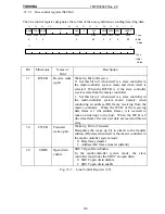
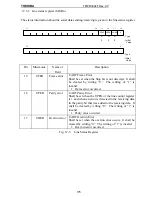
When a parity bit is attached to a 7-bit length, the parity is shifted in to the 8th bit of the receive
shift register to be stored in the highest-order bit of the receive read buffer.
When a parity bit is attached to a 8-bit length, the parity is stored in the RWUB of the line
control register.
12.4.6 Receiver shift register
This is a 8-bit shift register. It shifts in such that the first data bit that was received is bit0 (the
lowest-order bit).
12.4.7 Receiver read buffer
This is a buffer placed between the receive shift register and the receive FIFO buffer. After
receiving a data frame, the data are stored in this buffer and a parity check is conducted.
12.4.8 Transmitter controller
When the transfer shift register has taken out all of the previous data, one data frame is taken
from the transfer FIFO buffer to the transfer shift register. 1 bit is sent out every SIOCLK 16
clocks.
12.4.9 Transmitter shift register
This is a 8-bit shift register. It shifts out from the lowest order-bit in due order to transfer data.
12.4.10 Host I/F
The sending data are written into the transfer FIFO buffer by the interrupt by the sending data
empty or the DMA transfer. The writing-in by the interrupt is conducted by the byte by the
CPU. Every time the read pointer of the transfer FIFO buffer changes, an interrupt is generated
to request the CPU for sending data. In the writing-in to the transfer FIFO buffer by the DMA
transfer, when sending data of 4 bytes or 8 bytes are sent to the transfer shift register (when the
read pointer (0-7) becomes 4 and 0), a DMA request is generated and the data for sending are
taken in from the memory.
The reading-out from the receive FIFO buffer is conducted by the interrupt process or the DMA
transfer. Every time 1-byte receiving data are written in to the receive FIFO buffer (i.e., every
time the write pointer of the receive FIFO buffer moves), an interrupt is generated and the CPU
reads out the data.
In the interrupt mode, the FIFO functions as a simple one stage buffer and makes up a double-
buffer with a read buffer.
Summary of Contents for TMPR3904F
Page 1: ...Users Manual 32bit RISC Microprocessor TX39 family TMPR3904F Rev 2 0 Jan 12 1998 ...
Page 2: ......
Page 9: ...Users Manual 01 1 INTRODUCTION 1 1 Overview ...
Page 11: ...Users Manual 03 1 3 Kind of accessing by the TX3904 ...
Page 12: ...Users Manual 04 1 4 Precautions in the TMPR3904F specification Don t set Don t use ...
Page 13: ...Users Manual 05 Do not use ...
Page 14: ...Users Manual 06 ...
Page 15: ...Users Manual 7 2 FEATURES n n n n n n n n n n n n n ...
Page 16: ...Users Manual 8 ...
Page 18: ...Users Manual 10 ...
Page 19: ...Users Manual 11 4 PINS 4 1 Positions of Pins ...
Page 20: ...Users Manual 12 ...
Page 21: ...Users Manual 13 4 2 Functions of Pins ...
Page 22: ...Users Manual 14 ...
Page 23: ...Users Manual 15 ...
Page 24: ...Users Manual 16 ...
Page 26: ...Users Manual 18 5 2 Register Map ...
Page 27: ...Users Manual 19 ...
Page 28: ...Users Manual 20 ...
Page 30: ...Users Manual 22 5 3 2 PIO2 and PIO1 ...
Page 32: ...Users Manual 24 5 3 4 Connection of external bus master 5 3 5 INT 7 0 active status clear ...
Page 33: ...Users Manual 25 5 3 6 INT 7 0 active status set up ...
Page 34: ...Users Manual 26 ...
Page 123: ...TOSHIBA TMPR3904F Rev 2 0 115 26 ...
Page 169: ...TOSHIBA TMPR3904F Rev 2 0 161 26 ...
Page 203: ...TOSHIBA TMPR3904F Rev 2 0 195 ...
Page 230: ......


