background image


16.2


SPECIFICATIONS 


As of the date this manual was published, the following specifications apply to all RFL 9785 
Checkback modules. Because all RFL products undergo constant refinement and improvement, these 
specifications are subject to change without notice. 


Codes:


Capable of transmitting and receiving 16 asynchronous codes (01 through 16) 


Test Log:


Available through RS-232 port or optional Checkback Alarm Chassis (See 
Section 20) 


Test/Fail Output:


Solid-state relay, rated for 1 ampere. 


16.3


TYPICAL CHECKBACK APPLICATION 


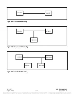
A two-terminal line (Figure 16-5a) can be programmed with the RFL 9785 to perform the test 
sequence shown in Figure 16-5b. The Master station will initiate the test automatically once every 24 
hours, starting 3 hours after the unit is programmed. Tests can also be initiated manually, or by 
external input. Each terminal is tested at both full-power and reduced-power levels, and each terminal 
can send a continuous carrier upon request from the other terminal (Figure 16-5c).  


STATION A


STATION B


MASTER


REMOTE


A. One-line diagram.


STATION A - MASTER


1


TX 01


RX 01


2


TX 02


RX 02


B. Checkback test routine.


STATION A


MASTER


HC 1


TX 03


RX 04


TX HC


TX 05


RX 06


TX HC


HIGH

HIGH

LOW

LOW

HIGH

HIGH

HIGH

HIGH

HIGH

LOW

STATION B - REMOTE


RX 01
TX 01

RX 02

TX 02

STATION B


REMOTE


RX 03
TX HC

TX 04

RX 05
TX HC

TX 06

C. Hard carrier request routines.


LOW

HIGH

HC 1


HC 2


HC 2


KEY:
TX 01     CODE SENT
RX 01     CODE RECEIVED


TX HC    HARD CARRIER SENT


TEST CODE OR HARD CARRIER REQUEST
HARD CARRIER


Figure 16-5.  Checkback testing of typical two-terminal system 

RFL 9785 


RFL Electronics Inc. 

July 26, 2007 

                         16-3 

(973) 334-3100 

Summary of Contents for 9785

Page 1: ...nless written permission is given by RFL Electronics Inc This manual has been compiled and checked for accuracy The information in this manual does not constitute a warranty of performance RFL Electronics Inc reserves the right to revise this manual and make changes to its contents from time to time We assume no liability for losses incurred as a result of out of date or incorrect information cont...

Page 2: ... one way shipping cost of the failed assembly to the RFL Customer Service facility in Boonton New Jersey RFL warrants product repair from one year from the date of repair or the balance of the original factory warranty whichever is longer This warranty does not apply if the equipment has been damaged by accident neglect misuse or causes other than performed or authorized by RFL Electronics Inc Thi...

Page 3: ...RY CAUTION FOR YOUR SAFETY THE INSTALLATION OPERATION AND MAINTENANCE OF THIS EQUIPMENT SHOULD ONLY BE PERFORMED BY QUALIFIED PERSONS WARNING RFL 9785 RFL Electronics Inc March 1 2013 iii 973 334 3100 The equipment described in this manual contains high voltage Exercise due care during operation and servicing Read the safety summary on the reverse of this page Warning Do not disconnect under power...

Page 4: ...i g n s a n ds p e c i fi c a t i o n s wi t h o u t n o t i c e WARNING POWER MUST BE TURNED OFF BEFORE REMOVING OR INSTALLING ANY RFL 9785 MODULES FAILURE TO DO SO MAY RESULT IN COMPONENT DAMAGE WARNING ON INITIAL INSTALLATION ENSURE THAT ALL MODULES ARE FULLY SEATED INTO CONNECTORS BEFORE POWERING ON UNIT RFL 9785 RFL Electronics Inc March 1 2013 iv 973 334 3100 ...
Page 5: ...priate protection measures must be taken Electrical shock can result in serious injury because it can cause unconsciousness cardiac arrest and brain damage Throughout this manual warnings appear before procedures that are potentially dangerous and cautions appear before procedures that may result in equipment damage if not performed properly The instructions contained in these warnings and caution...

Page 6: ... c o n t i n u o u s p r o d u c t i mp r o v e me n t wer e s e r v et h er i g h t t oc h a n g ed e s i g n s a n ds p e c i fi c a t i o n s wi t h o u t n o t i c e This page intentionally left blank RFL 9785 RFL Electronics Inc March 1 2013 vi 973 334 3100 ...

Page 7: ...EM THEORY OF OPERATION 2 10 Section 3 INSTALLATION 3 1 3 1 INTRODUCTION 3 1 3 2 UNPACKING 3 1 3 3 MOUNTING 3 2 3 4 VENTILATION 3 3 3 5 CONNECTIONS 3 4 Section 4 OPERATING INSTRUCTIONS 4 1 4 1 INTRODUCTION 4 1 4 2 FRONT PANEL CONTROLS AND INDICATORS 4 1 4 3 JUMPERS AND SWITCH SETTINGS 4 1 4 4 POWER SUPPLY CONSIDERATIONS 4 7 4 5 INPUT AND OUTPUT VOLTAGES 4 7 4 6 TRANSMIT FUNCTIONS 4 8 4 7 RECEIVER F...

Page 8: ...ILTER MODULES 10 1 10 1 DESCRIPTION 10 1 10 2 SPECIFICATIONS 10 2 10 3 THEORY OF OPERATION 10 3 10 4 CONTROLS AND INDICATORS 10 3 Section 11 RECEIVER DOWNSHIFTER MODULE 11 1 11 1 DESCRIPTION 11 1 11 2 SPECIFICATIONS 11 2 11 3 THEORY OF OPERATION 11 2 11 4 CONTROLS AND INDICATORS 11 5 Section 12 RECEIVER DETECTOR MODULE 12 1 12 1 DESCRIPTION 12 1 12 2 SPECIFICATIONS 12 2 12 3 THEORY OF OPERATION 12...

Page 9: ...BACK COMMUNICATIONS MODULE 17 1 17 1 INTRODUCTION 17 1 Section 18 POWER SUPPLY MODULE POWER SUPPLY I O MODULE 18 1 18 1 INTRODUCTION 18 1 18 2 POWER SUPPLY MODULE 18 2 18 3 POWER SUPPLY I O MODULES 18 13 Section 19 I O MODULES 19 1 19 1 INTRODUCTION 19 1 19 2 SOLID STATE INPUT I O MODULE 19 3 19 3 SOLID STATE INPUT OUTPUT I O MODULE 19 11 19 4 ALARM RELAY I O MODULE 19 23 19 5 RF LINE I O MODULE 1...

Page 10: ... 4 Figure 8 3 Schematic RFL 9785 Power Amp Dwg No C 106464 C 8 6 Figure 9 1 RFL 9508 RF Chassis Front Views 9 1 Figure 9 2 Front View of RFL 9508 RF Chassis 9 2 Figure 9 3 RFL 9508 RF Chassis Block Diagram 9 3 Figure 9 4 RFL 9508 Power Amplifier 9 5 Figure 9 5 RFL 9508 Power Amplifier Power Supply 9 7 Figure 9 6 9508 Power Amplifier Power Supply Block Diagram 9 8 Figure 9 7 Tx Filter Top View 9 9 ...

Page 11: ...d panel views of RFL 9785 SOE IRIG B I O module 13 11 Figure 13 5 Controls and indicators for the RFL 9785 SOE IRIG B I O module 13 12 Figure 13 6 Schematic RFL 9785 SOE IRIG B I O Dwg No D 106479 B 13 13 Figure 14 1 Making connections from the PC to the RFL 9785 front cover 14 1 Figure 14 2 Making connections from the PC to the RFL 9785 rear connector 14 2 Figure 14 3 APRIL main menu 14 3 Figure ...

Page 12: ...L 9785 19 1 Figure 19 2 Solid State Input I O module rear panel view 19 3 Figure 19 3 Controls and indicators Solid State Input I O modules 19 5 Figure 19 4 Schematic RFL 9785 Solid State Input I O Dwg No D 106439 3 A 19 7 Figure 19 5 Schematic RFL 9785 Solid State Logic Level Input I O Dwg No D 106439 5 B 19 9 Figure 19 6 Typical Solid State Input Output I O module rear panel view 19 11 Figure 19...

Page 13: ...nt Panel 4 3 Table 4 2 Controls and indicator information for RFL 9785 system modules 4 4 Table 4 3 Input Attenuator Settings 4 14 Table 5 1 Fuse replacement data RFL 9785 Power Supply I O Modules 5 5 Table 6 1 Controls and indicators RFL 9785 AM Logic Module 6 6 Table 6 2 Switch Settings DIP Switch SW1 6 7 Table 6 3 Switch Settings DIP Switch SW1 6 7 8 6 7 Table 6 4 Switch Settings DIP Switch SW2...

Page 14: ...e 18 4 Controls and indicators RFL 9785 Single Power Supply I O module 18 14 Table 18 5 Controls and indicators RFL 9785 Dual Power Supply I O module 18 17 Table 18 6 Controls and indicators RFL 9780 85 External Amp Power Supply I O module 18 21 Table 19 1 RFL 9785 I O modules Application Information 19 2 Table 19 2 Controls and indicators Solid State Input I O module 19 4 Table 19 3 Solid State I...

Page 15: ...anual dated March 1 2013 the sections are dated as follows Front Matter March 1 2013 Section 1 March 2005 Section 2 June 18 2009 Section 3 May 16 2011 Section 4 March 24 2008 Section 5 April 25 2005 Section 6 February 7 2007 Section 7 April 25 2005 Section 8 September 1 2006 Section 9 May 16 2011 Section 10 June 18 2009 Section 11 June 18 2009 Section 12 July 7 2006 Section 13 December 7 2009 Sect...

Page 16: ...ce with RFA number 7005 6 26 00 CS 7 5 00 Revised in accordance with ECO numbers 9785 026 028 Revised in accordance with ECO numbers 9780 046 047 059 7 28 00 CS 11 8 00 Revised in accordance with ECO number 9785 033 Added new Section 16 Checkback Comms Module Added new Section 20 Checkback Alarm Chassis Added new SS I O modules 106635 1 2 3 and 4 12 8 00 CS 3 31 01 Revised in accordance with ECO n...

Page 17: ...85 030 Voice Module 9785 041 AM Logic and Motherboard 9785 044 Rx Detector 9785 046 Rx Detector 9785 052 RF Line I O 9785 053 Voice Filter 9785 054 Checkback 9785 055 Checkback revise U7 9785 056 Rx Detector 9780 101 add C15 C22 to CLI 9780 109 9785 I Os 9780 116 CLI R97 from 1 5K to 1K R99 from 10K to 499Ω 9780 129 Release SOE Output Filters with RPM 9780 131 Add R58 R59 to 48 125 add C61 C62 to ...

Page 18: ...porate errata sheet MC 9780 001 in accordance with ECO 9780 146 and CAR C9780 0121 Incorporate errata sheet MC 9780 003 in accordance with ECO 9780 150 Incorporate errata sheet MC 9780 007 in accordance with CAR C9780 0136 Revised in accordance with CAR C9785 0051 Incorporate errata sheet MC 9780 003 B in accordance with CAR 9780 0138 1 16 04 CS 6 16 04 Incorporate errata sheet MC 9785 002 in acco...

Page 19: ...corporated errata sheet MC9785 013 in accordance with ECO No 9780 187 Incorporated errata sheet MC9785 014 in accordance with CAR C9780 0184 Incorporated errata sheet MC9785 015 in accordance with ECO No 9780 189 Incorporated errata sheet MC9785 016 in accordance with ECO No 9508 049 Incorporated errata sheet MC9785 017 in accordance with ECO No 9780 186 Incorporated errata sheet MC9785 018 in acc...

Page 20: ...34 3100 REVISION RECORD continued 6 18 09 Revise the Commissioning Section 22 and add commissioning and test procedures for a 50 100 watt system using the 9508 RF chassis Minor updates to body of manual 6 18 09 TG 11 1 10 Update Section 9 as per ECO9508 113 9508 RF Chassis Power Amp Circuit Board Changes 11 1 10 TG 5 16 11 Important grounding update in Section 3 Update to Section 9 as per ECO9508 ...

Page 21: ...me n t wer e s e r v et h er i g h t t oc h a n g ed e s i g n s a n ds p e c i fi c a t i o n s wi t h o u t n o t i c e RFL 9785 RFL Electronics Inc September 1 2006 1 1 973 334 3100 Section 1 PRODUCT INFORMATION Please see the following page for the Product Information Sheet 1 9785 Product Information sheet ...

Page 22: ... o n t i n u o u s p r o d u c t i mp r o v e me n t wer e s e r v et h er i g h t t oc h a n g ed e s i g n s a n ds p e c i fi c a t i o n s wi t h o u t n o t i c e This page intentionally left blank RFL 9785 RFL Electronics Inc September 1 2006 1 2 973 334 3100 ...

Page 23: ...atible with almost every existing carrier blocking relay One standard package is all RFL 9785 Programmable ON OFF Powerline Carrier System Complies to ANSI C93 5 Standard Integrated Sequence of Events Option Integrated Reflected Power Meter Option Key Features and Benefits you will need for most schemes A complete 10 watt transmitter receiver is contained in a 19 inch chassis that occupies three r...

Page 24: ...fits and Features 2 Optional SOE IRIG B Reflected Power Measurement Module The major status signals within the chassis are constantly monitored by a sequence of events SOE module Table 1 This module detects and records any changes in the system status The SOE log may be downloaded via an RS 232 con nection both front and rear connections standard to provide a time and date stamped record of events...

Page 25: ...re recalled most recent event first The forty most re cent events are retained The local clock is automatically syn chronized to an externally supplied IRIG B signal if available IRIG B input 1000 Hz modulated or direct TTL Signals monitored See Table 1 Output Ratings Solid State Outputs Maximum continuous current 1Amp Maximum 1 minute current 2 Amps Maximum 100 mSec current 10 Amps Maximum open c...

Page 26: ... outputs are available Figure 1 Typical RFL 9785 Programmable ON OFF Powerline Carrier System Block Diagram Two Wire Operation The RF transmitter output and receiver input are jumpered together with two UHF connectors J5 and J7 Either con nector can be connected to the line tuning equipment This provides a maximum continuous output power of 10 Watts with a nominal input output impedance of 50 Ohms...

Page 27: ...c yo f c o n t i n u o u s p r o d u c t i mp r o v e me n t wer e s e r v et h er i g h t t oc h a n g ed e s i g n s a n ds p e c i fi c a t i o n s wi t h o u t n o t i c e Figure 2 Typical Rear View RFL 9785 Programmable ON OFF Powerline Carrier System ...

Page 28: ...f UNlf auwur PA LL S I TAELC I TBl 3 r T fBL 7 R3 t06510 x 6 301009 5 DB L5 mu I I I T84 7 tt I I rnJ 1 I BLOCK BLOCK _ UTPUf TBJ 2 RECE_C_V_E_D BLOCK f t B c L c OC K ___ OUTPUT 2 l RECE V D l fK BK AUX 1 I CHASS S L06635 L Q65 i 6 SOE RS 232 _ ON FRONT nmR soc 06480 soc 1 IJ IG B 10611 i 2 RX DE L065L5 X OJrPur Ll653D X VOCC va C f RO T f HEI_ 6 6 NOTES 0 ND CAfES fERl t NAL BLOCK CDNNECnDN ON R...

Page 29: ... t i c e RFL Electronics Inc March 2005 RFL 9785 The RFL 9785 ON OFF Powerline Carrier can be configured for either 50 or 100 Watt RF power outputs The RFL Model 9508 RF power amplifier is rated for 50 Watt PEP and is the standard amplifier used for single sideband applications Two amplifiers are required for 100 Watt applications Figure 4 RFL 9785 50 Watt Configuration 7 Specifications subject to...

Page 30: ...r o v e me n t wer e s e r v et h er i g h t t oc h a n g ed e s i g n s a n ds p e c i fi c a t i o n s wi t h o u t n o t i c e RFL Electronics Inc March 2005 RFL 9785 RFL Electronics Inc 353 Powerville Road Boonton Twp NJ 07005 P 9 7 3 3 3 4 3 1 0 0 F 9 7 3 3 3 4 3 8 6 3 w w w r f l e l e c t c o m ...

Page 31: ...columns A and C and provide a total of 64 pins per connector In addition to this the AM Logic Module has pins in column B giving an additional 32 pins for a total of 96 pins Note that the pins extend from the front to the back of the unit into the I O Module connector The I O connector pins are a mirror image of the front connector pins In order to clarify signal flow the signal on pin 1 of a fron...

Page 32: ...l is shown in Figure 2 1 WARNING MANY OF THE CIRCUITS IN THE RFL 9785 ARE FACTORY TUNED ACTIVE CIRCUITS NONE OF THE PARTS IN THESE CIRCUITS ARE FIELD REPLACEABLE UNAUTHORIZED MODIFICATIONS OR ALTERATIONS TO THESE CIRCUITS WILL COMPROMISE SYSTEM PERFORMANCE 2 2 PURPOSE OF EQUIPMENT The RFL 9785 is an amplitude modulated ON OFF powerline carrier transmitting and receiving terminal It is an enhanced ...

Page 33: ... through optically isolated high current transistors electro mechanical output relays or both Compatibility With Existing Equipment The RFL 9785 is backwards compatible with existing RFL 6785P units as well as almost every other existing directional comparison blocking relay presently in the field Carrier Level Indicator The RFL 9785 continuously monitors incoming carrier level with a digital pane...

Page 34: ...d Because all RFL products undergo constant refinement and improvement these specifications are subject to change without notice 2 5 1 TRANSMITTER SECTION Frequency Range 30 kHZ to 535 kHz switch selectable in 10 Hzsteps Modulation ON OFF amplitude modulated and optional voice modulated Frequency Stability 10 Hz crystal controlled Output Power 10 watts measured at the amplifier output Additional p...

Page 35: ... isolated from ground and from all other circuits Breakdown is 1500 Vrms 50 60 Hz 2500 Vdc and 2500 Vrms 1 5 MHz in accordance with IEEE Surge Withstand Capability Specification 472 1978 ANSI C 37 90 1978 The RFL 9785 also meets the requirements of ANSI IEEE Fast Transient Specification C 37 90 1 1988 Input Power Requirements Voltage Range 48 Vdc Systems 40 Vdc to 58 Vdc 125 Vdc Systems 103 Vdc to...

Page 36: ...6515 6 7 8 F Section 12 Voice Filter Plug On 106580 2 Section 15 2 Seq Of Events IRIG B Module 106480 1 F Section 13 Seq Of Events IRIG B I O 106475 2 R Voice Module 106565 F Section 15 Checkback Module 106525 F Section 16 Checkback Communications Module 106645 F Section 17 Power Supply 48 125 Vdc 250 Vdc Power Supply I O 48 125 Vdc 250 Vdc Dual Power Supply I O 48 125 Vdc 250 Vdc 106535 1 106535 ...

Page 37: ...everal circuit board modules and I O modules Paragraphs 2 7 1 through 2 7 12 describe the different modules used in the RFL 9785 terminal 2 7 1 AM LOGIC MODULE The 9785 AM Logic Module monitors the CARRIER START CARRIER STOP and RESERVE KEY keying inputs as well as signals from other modules of the RFL 9785 It uses this information to generate command signals for the transmitter and receiver detec...

Page 38: ... the 50 and 100 Watt PowerAmplifers used with the RFL 9785 see Section 9 2 7 5 OUTPUT FILTER MODULES RFL 9785 Output Filter modules are used to reduce the harmonic content of the Power Amplifier s output signal to a level that is at least 55 dB below the carrier level In order to cover the RFL 9785 s entire operating range 30kHz to 535 kHz there are four different RFL 9785 Output Filters Three fil...

Page 39: ...sor based checkback system Control and logic signals are interfaced between the Checkback Module and the RFL 9785 system through the system mother board The Checkback Module is also connected to the SOE Module through the system motherboard The user can communicate with the Checkback Module by using the RS 232 connector located on the RFL 9785 front panel or by using the RS 232 connector located o...

Page 40: ...e 2 2 2 8 1 TRANSMITTER SECTION The function of the transmitter section is to provide the desired carrier frequency at the desired power level at the transmitter port when commanded The transmitter consists of three basic modules the Transmitter Module the Power Amplifier Module and the Output Filter Module The Transmitter Module generates a clean precise carrier at the desired frequency and at a ...

Page 41: ...ic Module The received signal enters the 9785 chassis through a Line I O Module The Line I O module has two UHF connectors screw type terminal connections impedance matching circuits and ANSI C 37 90 compliant protection circuits See Section 18 for additional information regarding the Line I O module The signal is then fed to the Downshifter Module This module normalizes the received level and shi...

Page 42: ...r is intended for short term connection to a PC or terminal for system interrogation The front connector input overrides the rear connector The user may request the present status of the 9785 chassis on a one time or continuous update basis Additionally the module saves the forty most recent changes in status in a log with time and date stamping This data may be viewed or downloaded one record at ...

Page 43: ...as individual chassis or interconnected with other chassis or assemblies as part of a system Paragraph 3 2 1 provides unpacking instructions for individual chassis and paragraph 3 2 2 provides instructions for interconnected chassis 3 2 1 INDIVIDUAL CHASSIS RFL 9785 terminals supplied as individual chassis are packed in their own shipping cartons 1 Open each carton carefully to make sure the equip...

Page 44: ... be securely mounted following the instructions in paragraphs 3 3 1 through 3 3 3 3 3 1 INDIVIDUAL CHASSIS RFL 9785 terminals housed in individual chassis have two mounting ears one on each side Hole sizes and spacings conform with EIA standards so the RFL 9785 can be mounted in any standard 19 inch rack or cabinet Complete chassis dimensions are shown in Figure 3 1 CAUTION ANY INSTALLATION USING ...

Page 45: ...abinet as possible with the rear panels of the equipment facing the front of the rack or cabinet 2 Remove all the screws securing the shipping rails to the equipment 3 Slide the equipment into the rack or cabinet 4 Install and tighten screws to all panels to secure the equipment in place 3 4 VENTILATION The specified operating temperature range for RFL 9785 equipment is 20o C to 60o C 4o F to 140o...

Page 46: ...ires to the terminal blocks proceed as follows 1 Remove the transparent protective cover from the rear of the chassis by loosening the mounting screws and sliding the panel up and off of the standoffs holding it in place 2 Using strippers remove about 1 4 inch 10 cm of insulation from the end of the wire to be connected 3 If local practice calls for lugged wires crimp a spade lug onto the stripped...

Page 47: ... 5 3 SOLID STATE OUTPUT CONNECTIONS Solid state output connections are made to terminal block TB3 on the rear of the RFL 9785 chassis Terminal assignments are shown below Be sure to observe proper polarity when making these connections Signal Name Positive Negative SS BLOCK 1 TB3 1 TB3 2 SS BLOCK 2 TB3 3 TB3 4 3 5 4 RELAY OUTPUT CONNECTIONS Relay output connections are made to terminal blocks TB4 ...

Page 48: ...PUT CONNECTIONS Checkback output connections are made to terminal block TB8 on the rear of the RFL 9785 chassis Terminal assignments are as follows Signal Name Contact Type Terminal Assignments CHECKBACK TIP COMMON TB8 1 NORMALLY OPEN TB8 2 NORMALLY CLOSED TB8 3 CHECKBACK FAIL COMMON TB8 4 NORMALLY OPEN TB8 5 NORMALLY CLOSED TB8 6 The Checkback TIP Test In Progress relay and the Checkback Fail rel...

Page 49: ...WARNING THE RFL 9785 CHASSIS MUST BE PROPERLY GROUNDED AS DESCRIBED IN THE FOLLOWING PARAGRAPH BEFORE ATTEMPTING TO CONNECT INPUT POWER IMPROPER GROUND CONNECTIONS MAY RESULT IN SYSTEM MALFUNCTIONS EQUIPMENT DAMAGE OR ELECTRICAL SHOCK 3 5 10 CHASSIS GROUND CONNECTIONS A threaded ground stud at the rear lower right of the RFL 9785 chassis is the main ground for the RFL 9785 terminal Grounding is ac...

Page 50: ...ns have been made to the RFL 9785 power connections can be made The terminal battery voltage is connected to terminal block TB10 positive to TB10 1 and negative to TB10 2 Depending on the dc dc converter power supply installed in the terminal either 48 volt or 125 volt terminal batteries can be accommodated A switched station battery output is also available on terminal block TB10 positive at TB10...

Page 51: ...OCK RELAY 2 COM TB5 5 BLOCK RELAY 2 NO TB5 6 BLOCK RELAY 2 NC TB5 7 BLOCK RELAY CONNECTIONS EXTERNAL CARRIER RECEIVE LEVEL METER CONNECTIONS METER TB9 7 METER TB9 8 CONNECTIONS CARRIER TRANSMIT AND RECEIVE CHASSIS GROUNDING STUD 8 LUG TRANSMIT NORMALLY INTERNALLY CONNECTED TO RECEIVE RECEIVE NORMALLY INTERNALLY CONNECTED TO TRANSMIT UHF SIG GND UHF SIG GND J5 TB9 1 TB9 2 J7 TB9 5 TB9 6 POWER FAIL ...

Page 52: ...ontinuous service 4 2 FRONT PANEL CONTROLS AND INDICATORS The front panel of the RFL 9785 terminal contains controls and indicators which are used to monitor system functions during normal operation These controls and indicators are shown in Figure 4 1 and are described in Table 4 1 Module locations for the front and rear panels are shown in Figure 4 2 4 3 JUMPERS AND SWITCH SETTINGS Most RFL 9785...

Page 53: ...e c i fi c a t i o n s wi t h o u t n o t i c e POWER RX DETECT BLOCK OUT START INPUT STOP INPUT RESERVE INPUT REMOTE INITIATE TX CARRIER ON TX FAIL RFL 9785 Programmable ON OFF Powerline Carrier System RFL Electronics Inc SOE RS 232 RECEIVE dB 1 2 3 4 5 6 7 8 9 10 11 Figure 4 1 Controls and indicators RFL 9785 front panel RFL 9785 RFL Electronics Inc March 24 2008 4 2 973 334 3100 ...

Page 54: ...PUT indicator Lights red when CARRIER START input is active 4 BLOCK OUT indicator Lights red when a block condition has been detected 5 RX DETECT indicator Lights red when a received signal has been detected 6 RECEIVE LEVEL display Displays the power level of the received carrier signal in dB The range is 10 dB to 10 dB 7 SOE RS 232 connector Allows a user to view the SOE log using a dumb terminal...

Page 55: ...gure 10 2 10 Receiver Downshifter module Table 11 1 Figure 11 3 11 Receiver Detector module Table 12 1 Figure 12 3 12 SOE IRIG B module Table 13 1 Figure 13 2 13 SOE IRIG B I O module Table 13 3 Figure 13 5 13 Voice module Table 15 1 Figure 15 3 15 Checkback module Tables 16 1 16 2 Figures 16 7 16 8 16 Power supply module Table 18 2 Figure 18 2 18 Power supply I O module Tables 18 4 18 5 Figures 1...

Page 56: ...68 2 SPACES CHECKBACK SOE 14 768 15 968 SOE BLANK 9785 SS I O SS INPUT ALARM RELAY 9785 RF LINE I O RX J7 TX J5 PA 19 SB 4A F1 SW SB SW SB P S I O O I OFF SB ON 180mA 1 AMP 200mA 1 SB 6 7 20mA 5 4 3 2 RLY RLY CURRENT TB1 1 1 1 IRIG B VOICE MIC EAR CALL KEY REV D CALL 12V RET 5 6 TB2 3 4 RS 232 COM 2 1 BLOCK 2 SS 4 2 3 6 NO 6 NO 7 RLY1 BLOCK NC BLOCK NC RLY2 7 STOP 4 5 C 3 2 START RMT INIT C 5 4 RE...

Page 57: ...l Power Supply I O and two 106535 2 250 Vdc Power Supplies See section 16 for more information on the power supplies and power supply I Os There are other power supply configurations that may be appropriate under certain circumstances For example if more than 10 W of transmit power is required an external amplifier will be required and the external amplifier may be able to supply power to the 9785...

Page 58: ...ate the required carrier frequency There are three banks of direct reading rotary switches on the module The middle bank contains five switches which are used to set the center frequency of the system with 10 Hz resolution The other two banks of switches are used only in FSK systems See Section 7 for more information on the Transmitter Module 4 6 2 TRANSMIT POWER The system can be configured for a...

Page 59: ... To change the termination setting the Line I O Module must be removed from the chassis and the jumper selected for 50Ω 75Ω or OUT If the receive sections of several chassis are interconnected only one of them should be terminated Note that the termination impedance is only specified up to one watt maximum See Section 19 for more information NOTE In two wire operation Rx tied to Tx W3 and W5 short...

Page 60: ...eliable The AM logic module allows for a delay between the carrier being enabled and a transmitter fail alarm being issued This pick up delay may be set for 3ms 50ms 100ms or 150ms using switches SW1 6 and SW1 7 on the AM Logic module The figure below illustrates various fail and status conditions See paragraph 6 3 4 for more information Note All contacts shown in their deenergized state TB7 1 TB7...

Page 61: ... remote end This can be enabled or disabled using switch SW2 1 on the AM Logic module See paragraph 6 3 3 for more information It should also be noted that the same function is often accomplished by connecting the Tx and Rx ports of the unit by installing a jumper on the line I O module 4 7 6 RX VOICE LEVEL The system can be configured for high or low voice levels using switch SW2 2 on the AM Logi...

Page 62: ... of the line and the receiver must be adjusted for the actual receive signal level This section assumes that the equipment has been installed and configured for the required application in accordance with Section 3 and paragraph 4 3 Note that the modules in the 9785 are not hot pluggable The power to the chassis must be turned off prior to removing in or installing any modules 4 8 1 EQUIPMENT REQU...

Page 63: ...d source impedance of a device are matched the loaded output voltage is exactly one half of the unloaded output voltage the internal and external impedances form a 50 voltage divider This fact is used to set the amplifiers output impedance However the power amplifier is not able to supply twice the rated output voltage when configured for 10 W operation The output impedance is simulated by active ...

Page 64: ...gnal level There is a coarse attenuator and fine level adjustment for the receive level 4 8 3 1 Input Attenuator Adjust the input attenuator as follows 1 Set the input attenuator J1 on the Receiver Downshifter to 50 dB 2 With the system in place and the far end transmitting a 10W block signal measure the receive level using a FSVM The FSVM must be set to the frequency being transmitted by the far ...

Page 65: ...HE TERMINAL BACK IN SERVICE 5 1 INTRODUCTION This section provides maintenance instructions for the RFL 9785 Topics discussed include removal and replacement procedures fuse replacement and corrective maintenance information Information is also provided on how to arrange for service by RFL personnel CAUTION EACH MODULE POSITION IN THE RFL 9785 CHASSIS IS DEDICATED TO A SPECIFIC MODULE TYPE AS INDI...

Page 66: ...pply module s will go out indicating that the terminal is turned off 3 Lower the lever at the front of the module until the module connector disengages with the motherboard connector 4 Slide the module out of the chassis To replace a circuit board module with the exception of the power supply module proceed as follows 1 Using the label along the front of the chassis as a guide determine the slot i...

Page 67: ...ule until the module connector disengages with the motherboard connector 5 Slide the module out of the chassis To replace the power supply module proceed as follows 1 Using the label along the front of the chassis as a guide determine the slot in the chassis where the power supply is to be installed Power supply modules can only be installed in the two left hand slots of the 9785 chassis 2 Line up...

Page 68: ... module to be removed Tag all wires before removal This will simplify rewiring once the I O module is replaced 4 Using a phillips head screw driver remove the two screws that hold the I O module in place 5 Pull the I O module out of the chassis To replace an RFL 9785 I O module proceed as follows 1 Using the label on the rear plastic panel as a guide determine the slot in the chassis where the I O...

Page 69: ...ltage is present and the power supply does not function troubleshoot the supply to determine the cause of failure 4 Insert a fuse with the proper voltage and current ratings into the fuseholder cap and push it in until it is firmly seated Using a flat blade screwdriver push in on the cap and turn clockwise about one quarter turn This will secure the fuse in place For continued safe operation alway...

Page 70: ... use the schematics at the end of Sections 6 through 21 to try and determine which module is defective Once this is done replace the module this should solve the problem Defective modules can be repaired locally or they can be returned to RFL for repair para 5 6 5 5 EXTENDER CARD Most RFL 9785 modules have test points which can be monitored when the module is mounted on an extender card The RFL pa...

Page 71: ...g to the requirements of the specific application The 9785 AM Logic Module also provides status information for the Sequence of Events Module SOE The 9785 AM Logic Module has eight red indicator lamps DS1 through DS 8 on the front edge of the module which protrude through the front panel of a closed chassis for ease of visibility These include RX DETECT DS1 BLOCK OUT DS2 START DS3 STOP DS4 RESERVE...

Page 72: ... the application An active START input will generate a logic high output signal unless the STOP is active A STOP command has priority over a START command The resulting logic high output is combined with other possible sources of carrier start These include DIRECT KEY TEST SWITCH SW12 RESERVE KEY and CHECKBACK KEY Any of these will generate a logic low SEND signal initiating carrier start START in...

Page 73: ... local carrier is active Voice is enabled by switch SW1 5 if the voice option is installed Voice will only be transmitted when SEND is not active The AM ENABLE signal at edge connector pin B24 will be a logic high when voice is being modulated over the carrier frequency 6 3 4 TRANSMITTER FAIL CIRCUIT The Transmitter Fail Circuit can be configured by switches SW1 6 SW1 7 and SW1 8 for 3ms 50ms 100m...

Page 74: ...inputs to the 9785 AM Logic Module will be logic low Both signals in the logic low state will generate a logic low POWER signal to prevent a BLOCK function for the period of the under voltage condition plus an additional 320ms The status of the block output circuit is monitored by the optional sequence of events module SOE 6 3 7 RECEIVE VOICE CONTROL LOGIC If the voice option is installed voice ca...

Page 75: ...lock diagram AM Logic Module DIRECT KEY C29 5 5 ART B21 OP C22 SW1 1 SW1 2 START DS3 STOP DS4 START OUT B26 STOP OUT A26 RESERVE OUT A15 UTILITY B27 SEND SW1 3 SW1 4 OSC 12 A13 OSC 3 B13 A SWITCH A14 B SWITCH B14 SW1 5 SW1 6 SW1 7 SW2 1 BLOCK OUT RLY1 C20 BLOCK OUT RLY2 B22 BLOCK OUT SS1 A22 BLOCK OUT SS2 C23 BLOCK OUT DS2 VOICE HIGH C27 VOICE LOW C25 VOICE MUTE A27 32 KHz POWER FAIL A17 CHECKBACK...

Page 76: ...the power amplifier has failed DS9 to DS16 LED indicators Not installed SW1 DIP Switch See Table 6 2 SW2 DIP Switch See Table 6 4 SW3 to SW10 DIP Switch Not installed SW11 Push button switch Not installed SW12 Toggle Switch Test switch used to manually key the transmitter module during setup and alignment as follows SW12 UP Enabled initiates local carrier DOWN Disabled TP1 Test point Monitoring po...

Page 77: ...ettings DIP Switch SW1 6 7 8 SW1 6 OFF DOWN OFF DOWN ON UP ON UP OFF DOWN OFF DOWN ON UP ON UP SW1 7 OFF DOWN ON UP OFF DOWN ON UP OFF DOWN ON UP OFF DOWN ON UP SW1 8 OFF DOWN OFF DOWN OFF DOWN OFF DOWN ON UP ON UP ON UP ON UP Normal Delay 3mspu 2 5msdo 50mspu 2 5msdo 100mspu 2 5msdo 150mspu 2 5msdo X4 Delay 12mspu 2 5msdo 200mspu 2 5msdo 400mspu 2 5msdo 600mspu 2 5msdo mspu millisecond pick up ms...

Page 78: ...P ON UP SW2 8 OFF DOWN ON UP OFF DOWN ON UP OFF DOWN ON UP OFF DOWN ON UP Block Hold Timer 0ms Default Setting 4ms 8ms 12ms 16ms 20ms 24ms 28ms Application Notes When using the 9785 Checkback feature the Block Hold Timer MUST be set for 0ms The Checkback data bits track the Block Output As such they are also extended by the same amount as defined by the Block Hold Timer This will adversely affect ...

Page 79: ...C8 C24 C20 C29 C17 C25 C26 C28 C27 C3 1 C32 C3 0 C5 C12 C14 C16 C15 CR7 TP 2 TP 1 CRZ1 CRZ5 CRZ8 CRZ4 CRZ3 CRZ7 CRZ6 S W 2 S W 5 S W 8 S W 4 S W 3 S W 7 S W 6 DS 1 DS4 DS5 DS6 DS7 DS 8 DS3 TP 4 TP 6 TP 7 TP 8 TP10 TP 9 TP11 TP12 TP 5 TP15 TP14 TP 16 R34 R35 R32 R33 CR Z9 U8 R47 S W 9 CRZ10 U1 6 U1 2 R37 R36 C37 C36 C35 C34 C33 TP 19 TP 18 TP 20 TP 17 RZ3 U1 1 U1 4 RZ 4 DS14 DS15 DS 16 DS13 DS12 DS...

Page 80: ... o n t i n u o u s p r o d u c t i mp r o v e me n t wer e s e r v et h er i g h t t oc h a n g ed e s i g n s a n ds p e c i fi c a t i o n s wi t h o u t n o t i c e RFL 9785 RFL Electronics Inc February 7 2007 6 10 973 334 3100 This page intentionally left blank ...

Page 81: ...1 BLK OUT RLY3 BLK_OUT_SS1 BLK_OUT_SS1 CB RLY TX FAIL CBFAIL RLY RESERVE_OUT STOP_2 DIPSW1 DIPSW1 DIPSW1 DIPSW1 DIPSW1 DIPSW1 DIPSW1 DIPSW1 DIPSW1 DIPSW1 DIPSW1 DIPSW1 DIPSW1 DIPSW1 DIPSW6 DIPSW6 DIPSW6 DIPSW6 DIPSW6 DIPSW6 DIPSW6 DIPSW6 DIPSW6 DIPSW6 DIPSW6 DIPSW6 DIPSW6 DIPSW6 BLK OUT RLY1 CRL_0 CRL_0 DIPSW3 DIPSW3 DIPSW3 DIPSW3 DIPSW3 DIPSW3 DIPSW3 DIPSW3 DIPSW3 DIPSW3 DIPSW3 DIPSW3 DIPSW3 DIPS...

Page 82: ...P4 CARRIER_SW_OUT LM_SP3 VOICE REQ IN SPARE IN2 SIG COMP IN UTILITY_OUT STOP 2 LM_SP2 DIRECT IN CHKBACK IN CB LEVEL IN POWERFAIL 2 LM_SP1 CBFAIL IN VOICE_MUTE SPARE OUT2 SPARE OUT1 AM EN CB TIP RMT INIT RESERVE_OUT AGND AGND AGND AGND AGND AGND AGND AGND START 2 STOP_2 CHKBACK_IN AM_EN SPARE_OUT2 SPARE_OUT1 CB_TIP SPARE_OUT3 UTILITY OUT STOP CARRIER SW OUT VOICE LOW VOICE MUTE RLYGND RLYGND CB_LEV...

Page 83: ...verter by reading a sine look up table stored in ROM If the voice option is installed in the system the output of the DDS is amplitude modulated to the audio signal input The output of the DDS is fed into an anti aliasing filter and the signal level is adjusted to achieve the desired overall transmission power 10W 3W or 1W output of the power amplifier The desired output frequency is selected by p...

Page 84: ...o constant refinement and improvement these specifications are subject to change without notice Output Frequency 30 kHz to 535 kHz adjustable in 10 Hz increments Frequency Stability 10 Hz Harmonic Content Less than 55 dB Output Range when used with RFL 9785 Power Amplifier Module 10 Watt Output 6 0 Vp p 3 Watt Output 3 4 Vp p 1 Watt Output 2 0 Vp p Voice Input 1 6 Vp p nominal a 1000 Hz test tone ...

Page 85: ...the input to the look up table is incremented the output of the table via the D A generates the sine wave Thus the input to the look up table is related to the phase of the output sine wave The phase information is stored in the phase register 7 3 1 DIRECT DIGITAL SYNTHESIZER FUNDAMENTALS A simplified block diagram for a basic DDS is shown in Figure 7 3 The circuit has two inputs a master clock an...

Page 86: ...t Resistors R3 and R4 are used for current to voltage conversion U3C is configured as a differential amplifier to convert the output of U1 to a single ended signal 7 3 3 VOICE AMPLITUDE MODULATION When the voice option is installed U2A is used to modulate the reference input to the D A portion of the DDS based upon the voice input This varies the full scale setting of the D A thus providing the de...

Page 87: ...visible with the module installed in the chassis All other controls are only accessible when the module is removed from the chassis or is on a card extender RFL Part No 9547 1870 Table 7 1 Controls and indicators RFL 9785 Transmitter Module Component Designator Name Description Function DS1 Carrier Enabled LED Indicates the carrier is being generated DS2 Frequency 3 LED The carrier is set for shif...

Page 88: ...R25 R26 R27 R28 R29 R30 R31 DS 2 DS 3 DS 4 DS 5 DS 6 DS 7 DS 8 DS 9 C20 C2 C1 C15 C3 1 R1 8 TP 2 TP 3 TP 5 TP 4 TP 6 CR50 CR43 CR23 CR42 CR3 CR10 RZ1 RZ 2 S W 8 S W 9 S W 7 S W 5 S W 4 S W 3 CR2 S W 2 S W 1 TP 8 U7 R33 TP 7 199 9 RF L EL EC TR ON ICS IN C BO ON TO N NJ U S A EN UP FREQ DOWN SHFT CNTR SHFT C E NT E R FR E Q U E S HI FT U P 0 S HI FT D O W 0 978 0 8 5 TR AN SM ITT ER EC B NO 106 508...

Page 89: ...tary DIP switches arranged as 0 XX Khz SW1 and SW2 This allows the frequency to be set to within 10 Hz Only settings between 30 Hz and 535 Khz are valid 7 4 2 TRANSMIT AMPLITUDE POTENTIOMETER Potentiometer R23 is used to set the transmit amplitude of the module to achieve the proper output power while compensating for variations in installation and setup The system is normally set to a 10W output ...

Page 90: ...c o n t i n u o u s p r o d u c t i mp r o v e me n t wer e s e r v et h er i g h t t oc h a n g ed e s i g n s a n ds p e c i fi c a t i o n s wi t h o u t n o t i c e RFL Apri 9785 RFL Electronics Inc l 25 2005 7 8 973 334 3100 This page intentionally left blank ...

Page 91: ... OSC_3 CARRIER_EN 3 1W 3 1W VOICE_EN EN_AUDIO 1 8 1W 1 8 1W RESERVE_PWR RESERVE_PWR OSC_1 2 RESERVE SPARE_1 SPARE_2 PWR_B PWR_A STRSW_0 STRSW_1 STRSW_5 STRSW_6 STRSW_7 STRSW_8 12V_RELAY GUARD 15V 15V 15V VAR 10 DVDD_A DVDD_B DVDD_C DVDD_D AVDD_A AVDD_B DGND_A DGND_B DGND_C AGND_A AGND_B AGND_C AGND_D SLEEP REFIN REFOUT FSADJUST COMP IOUT IOUT RESET WR MCLK FSELECT PSEL1 PSEL0 DB0 DB1 DB2 DB3 DB4 D...

Page 92: ... CR41 CR42 CR3 CR4 CR5 CR6 CR7 CR8 CR9 CR10 5V STRSW_2 STRSW_4 STRSW_3 DIPSW2 DIPSW2 DIPSW2 DIPSW2 DIPSW2 DIPSW2 DIPSW2 DIPSW8 DIPSW8 DIPSW8 DIPSW8 DIPSW8 DIPSW8 DIPSW7 DIPSW7 DIPSW7 DIPSW7 DIPSW7 DIPSW7 DIPSW6 DIPSW6 DIPSW6 DIPSW6 DIPSW6 DIPSW6 DIPSW5 DIPSW5 DIPSW5 DIPSW5 DIPSW5 DIPSW5 DIPSW1 DIPSW1 DIPSW1 DIPSW1 DIPSW1 DIPSW1 DIPSW1 DIPSW4 DIPSW4 DIPSW4 DIPSW4 DIPSW4 DIPSW4 DIPSW4 DIPSW3 DIPSW3 ...

Page 93: ...t gain to the signal coming from the Transmitter module Section 7 A monitor circuit detects loss of transmit signal and issues a Transmitter Fail Alarm The output of the amplifier is transformer isolated and presents a 50 ohm nominal impedance The output impedance is adjustable to compensate for small changes in load impedance For specific component information at the board level please contact th...

Page 94: ...185 Ω typical Output Ratings Power 10 Watts rms continuous 50 Ω load Voltage 22 36 Volts rms Current 447 ma rms Impedance 50 Ω Frequency Response 30 to 535 Khz Total Harmonic Distortion 42 dB maximum typical 46 dB 10W rms Input Voltage Versus Power Out See table below 50 Ω load OUTPUT INPUT POWER WATTS RMS VOLTS PEAK VOLTS RMS VOLTS PEAK VOLTS RMS 10 9 8 7 6 5 4 3 2 1 31 62 30 00 28 28 26 46 24 49...

Page 95: ...controlled by current feedback provided by sense resistor R18 and input resistor R17 fixed and R16 variable The voltage developed across R18 is proportional to the load current and when combined with voltage feedback the amplifier s virtual output impedance can be determined Resistors R5 and R6 provide current limiting to protect the power operational amplifier from over current conditions Output ...

Page 96: ... are accessible with the RFL 9785 Power Amplifier Module installed in the chassis Test points TP1 TP2 and TP3 are only accessible when the module is removed from the chassis or is on a card extender R10 R2 R16 C15 R1 7 R16 C R5 R2 C R6 C4 C2 C1 C5 R6 R3 R1 C3 C R3 R1 0 TP1 U1 C R4 R5 R4 C6 106463 2 REV C 1999 RFL ELECTRONICS INC USA C16 C17 C9 C14 C10 T1 C8 TP3 TP2 CR7 R18 C11 R15 R14 R13 R9 R8 R1...

Page 97: ...er The Transmit Amplitude adjustment on the Transmitter Module can also be used to vary the output level 8 4 2 OUTPUT IMPEDANCE The Power Amplifier Module has provisions for adjusting the unit s output impedance to compensate for variations in actual field installations This should only require setting upon initial installation or following system changes that impact the impedance the 9785 is driv...

Page 98: ... o u s p r o d u c t i mp r o v e me n t wer e s e r v et h er i g h t t oc h a n g ed e s i g n s a n ds p e c i fi c a t i o n s wi t h o u t n o t i c e Figure 8 3 Schematic RFL 9785 Power Amp Dwg No C 106464 D RFL 9785 RFL Electronics Inc September 1 2006 8 6 973 334 3100 ...

Page 99: ...9 1 INTRODUCTION The RFL 9508 RF Chassis for use with the 9780 9785 amplifies the rf outputs of the 9780 85 before they are passed to the line coupling equipment The RFL 9508 RF Chassis shown in Figure 9 1a develops 50 Watts PEP For100 Watt applications two 50 watt power amplifiers are required which are wired in parallel The 100 Watt configuration is shown in Figure 9 1b NOTE The 9780 85 Reflecte...

Page 100: ...s included in 9508 RF Chassis Module Assembly Number For Additional Information Refer To The Following Paragraphs 50W Power Amplifier 103085 9 2 1 Power Amp Power Supply 107250 4 5 9 2 2 Tx Filter 107825 9 2 3 Balance Board 107815 9 2 4 Dummy Balance Board 107870 9 2 4 Line Board 103090 1 9 2 5 Rx Filter 107820 9 2 6 Rx Connection Board 107820 1 9 2 7 Attenuator Board 107810 9 2 8 RF Mother Board ...

Page 101: ...IL COM PWR FAIL NO PWR FAIL NC 92V 30V GND TB1 1 TB1 2 TB1 3 TB1 4 TB1 5 92V 30V GND SIGNAL IN GND FAIL OUT SIGNAL OUT ADDITIONAL 3U CHASSIS FOR 100W SYSTEMS ALARM ALARM RELAY_1 EXT AMP FAIL COM EXT AMP FAIL NC EXT AMP FAIL NO INT AMP FAIL COM INT AMP FAIL NC INT AMP FAIL NO FAIL GND FAIL GND BALANCE BOARD INPUT PORT 1 SIGNAL OUT INPUT PORT 2 INPUT SIGNAL OUT BALANCE TRANSFORMER INPUT SIGNAL OUT R...

Page 102: ... A green LED is located on the left side of the Power Amplifier front panel as shown in Figure 9 4 The LED is ON when the power amplifier is transmitting In those applications that require 100 Watts of RF output two 50 Watt Power Amplifiers are connected in parallel The second 50 Watt Power Amplifier is mounted in a 3U chassis directly above the RFL 9508 chassis as shown in Figure 9 1 There must b...

Page 103: ...hange without notice Number Of Inputs Four Input Level 4dBm 75 Ohms single input 1dBm 75 Ohms two inputs Input Impedance 75 Ohms nominal Idle Noise 65 dBmO measured in a 3 kHz bandwidth Frequency Response Flat within 2 0dB from 20kHz to 500 kHz Third Order Intermodulation Distortion From 60 to 350 kHz 60 dBmO Below 500kHz 50 dBmO Harmonic Distortion 40 dB Maximum Output 50 Watts PEP Output Resista...

Page 104: ...of Power Amplifier Power Supplies available as shown in Table 9 2 The 9508 Power Amplifier Power Supply is a dual output dc to dc converter It is a switching power supply using pulse width modulation The 107254 4 operates from 38 Vdc to 150 Vdc and the 107254 5 operates from 200 Vdc to 300 Vdc Each supply has two outputs 30 Vdc 0 25 Amps and 95 Vdc 2 4 Amps Both outputs are connected to a common g...

Page 105: ...0 4 38 Vdc to 150 Vdc 107250 5 200 Vdc to 300 Vdc Output Power 30 Vdc 0 25 Amps 92 Vdc 2 4 Amps RFL 9785 RFL Electronics Inc Operating Temperature 20o o o o C to 65 C 4 F to 149 F o Humidity 95 40 degC Isolation 2500 Vdc isolation from input terminals to ground output terminals to ground input terminals to output terminals relay contacts to ground and relay contacts to coil Dimensions 5 2 inches 1...

Page 106: ...onsisting of two PC boards and two air core inductors It plugs into the left side of the RF chassis as shown in Figure 9 2 The function of the Tx Filter is to filter out harmonics and noise that is out of the bandwidth of the filter The bandwidth of the filter can be set to either 8kHz or 16kHz using two programmable jumpers J1 and J45 The filter center frequency is tunable from 24kHz to 496kHz us...

Page 107: ...he board as shown in Figure 9 8 It plugs into the RF chassis just to the right of the Tx Filter as shown in Figure 9 2 The function of the Balance Board is to provide the capability of connecting two 50W Amplifiers in parallel for 100W applications In the event of one of the 50W Amps failing it sinks half of the power output of the remaining Power Amp The jumpers are used to select 50W or 100W ope...

Page 108: ...ssis and the Line Coupling equipment Because it contains no active components the Line Board does not require any dc input voltage 9 2 5 2 SPECIFICATIONS Power Capability 100 watts maximum Frequency Range 103090 20 500 kHz Impedances Transmit Input 50 ohms Receive Output 50 ohms Line Adjustable to 50 75 100 or 130 ohms Insertion Loss Transmit 1 5 dB maximum Receive 14 dB typical Input Power Requir...

Page 109: ...om the line coupling equipment can be monitored at TP2 9 2 5 3 2 RECEIVE ATTENUATOR Resistors R9 R11 R12 and dual section Receive Level potentiometer R10 are connected across the primary of T4 to form an attenuator The amount of signal sent to the Rx Filter is controlled by the setting of R10 Zener diodes CR1 and CR2 clamp the signal to a safe level The signal being sent to the RX Filter can be mo...

Page 110: ...equipment against an overvoltage condition Jumper J20 selects one of T2 s four impedance settings 50 75 100 or 130 ohms Fuse F2 provides current protection and surge arrestor E1 protects the equipment against an overvoltage condition In 2 wire applications the signal going to or coming from the line coupling equipment can be monitored at test point TP2 In 4 wire applications the signal going to th...

Page 111: ...RFL 9508 from the power line that is out of the bandwidth of the filter The bandwidth of the Rx Filter can be set to either 8kHz or 16kHz using two programmable jumpers on the board The filter center frequency is tunable from 24kHz to 496kHz using programmable jumpers The outer edges are 20kHz and 500kHz The 8kHz bandwidth is used for one or two RF channel operation and the 16kHz bandwidth is used...

Page 112: ... h t t oc h a n g ed e s i g n s a n ds p e c i fi c a t i o n s wi t h o u t n o t i c e 9 2 7 RX CONNECTION BOARD Figure 9 12 RFL 9508 Rx Connection Board 9 2 7 1 DESCRIPTION The Rx Connection Board is used in place of the Rx Filter in applications that do not require an Rx Filter RFL 9785 RFL Electronics Inc May 16 2011 9 15 973 334 3100 ...

Page 113: ...r Board 9 2 8 1 DESCRIPTION The RFL 9508 Attenuator Board consists of five 10 watt power resistors several other smaller resistors a two position toggle switch and two test points The function of the attenuator board is to provide 40dB of attenuation during loopback testing Toggle switch SW1 is used to select either Normal or Loopback operation Test points TP1 and TP2 allow the user to monitor the...

Page 114: ...o it from the front of the chassis which are the TX Filter Balance Board Line Board Attenuator Board Rx Filter Figure 9 14 shows the rear view of the motherboard Connectors J6 and J7 are TNC connectors which provide connections to the line coupling equipment J4 J5 J8 and J9 are BNC connectors J10 is a two pin plug in connector and TB1 is an eight position terminal block Table 9 3 Motherboard Rear ...

Page 115: ...al Amp Fail Relay COM TB1 5 External Amp Fail Relay NO TB1 6 External Amp Fail Relay NC TB1 7 Chassis Ground TB1 8 Earth Ground 9 2 9 2 GROUND CONNECTION AT TB1 8 At TB1 8 on the Mother Board Rear Panel a ground wire should be connected Ideally this wire should go directly to the sub station ground bar If this is not feasible shorting the wire to TB1 7 Chassis Ground is an alternate method This wi...

Page 116: ... 5 and Figures 9 2 and 9 15 A Typical RF Chassis will have modules installed as indicated in Figure 9 15 Table 9 5 Module Placement In RF Chassis 50W System Front Panel Modules Rear Panel Modules 50W Power Amplifier 9 3 1 Mother Board 9 3 8 Tx Filter 9 3 2 Power Amplifier Power Supply 9 3 9 Balance Board 9 3 3 Line Board 9 3 4 Rx Filter 9 3 5 Rx Connection Board 9 3 6 Attenuator 9 3 7 POWER AMP PO...

Page 117: ...dule which plugs into a slot in the RF Mother Board immediately to the right of the Balance Board 9 3 5 RX FILTER The Rx Filter is an optional module which plugs into a slot in the RF Mother Board immediately to the right of the Line Board In some applications it is used in place of the Rx Connection Board 9 3 6 RX CONNECTION BOARD The Rx Connection Board plugs into a slot in the RF Mother Board i...

Page 118: ...hown pictorially in Figure 9 16 Table 9 6 9508 RF Chassis Cables RFL cable part number From To Function 107806 2 of 2 J1 of Power Amp Power Supply J1 of Power Amp 3 conductor cable which provides dc power for Power Amp 107854 17 J2 of Power Amp J4 of Motherboard Coax high level output 107854 27 J2 of Motherboard J4 or J5 of Power Amp Coax low level input 107806 1 of 2 J3 of Power Amp J9 of Motherb...

Page 119: ...et h er i g h t t oc h a n g ed e s i g n s a n ds p e c i fi c a t i o n s wi t h o u t n o t i c e J1 Rear View Of Power Amp Power Supply Rear View of RF Chassis Motherboard Rear View of Power Amplifier J9 J4 J2 J1 J4 J2 J3 Figure 9 16 Cable connections in the RF Chassis RFL 9785 RFL Electronics Inc May 16 2011 9 22 973 334 3100 ...

Page 120: ...inimum 1U space between the lower 3U chassis and the upper 3U chassis for convection cooling The 3U chassis will contain a 50W Power Amplifier a Power Amp Power Supply a Tx Filter an External Amp Connection Board and a Motherboard The External Amp Connection Board has no components and consists only of a PC board and a motherboard connector A view of the additional 3U chassis is shown in Figure 9 ...

Page 121: ...Attenuator 9 6 5 Rx Filter 9 6 6 9 6 1 SETTING JUMPERS AND SWITCHES ON 50W POWER AMPLIFIER The 50W Power Amplifier has a circuit board which contains two programmable jumpers J6 and J7 In addition to this the board has five connectors J1 J2 J3 J4 J5 and five potentiometers R8 R14 R69 R74 R83 that must be set for proper system operation These components can be seen in Figure 9 18 on the following p...

Page 122: ...J3 DS1 SW1 SW2 Top View Switch Block Typical ON 1 2 3 4 SW2 5 6 7 8 RFL 9785 RFL Electronics Inc Figure 9 18 Circuit board of 50W Power Amp locations of jumpers connectors switches and potentiometers As shown above effective October 2010 two switch blocks have been added to the Power Amplifier Circuit Board These DIP switches are factory set to protect the circuit board from overvoltage or excessi...

Page 123: ...h set the outputs of the two 50W amplifiers 180 deg out of phase This will insure that the total output power is additive In 50W applications J6 and J7 can be set either way In 100W applications one 50W amp must be set to A and the other 50W amp must be set to B As a standard set the Main 50W amplifier to A and the Auxiliary 50W amplifier to B as shown below RFL 9785 RFL Electronics Inc J6 J7 Sett...

Page 124: ...et as follows Note that SW1 2 SW1 4 SW1 5 and SW1 6 are not used DIP Switch Phase Angle in Degrees RFL 9785 RFL Electronics Inc SW1 1 30 SW1 SW1 3 45 60 Default setting SW1 7 SW1 8 90 Phase Detector Set Point These DIP switches set the voltage threshold for the Phase Limit Setting The Phase limit circuit will not operate if the voltage falls below the preset SW2 1 through SW2 4 can be set as follo...

Page 125: ... two large air core inductors The location of these jumpers is shown in Figure 9 18 The remaining 17 Jumpers are located on the 107828 1 board The location of these jumpers is shown in Figure 9 19 Refer to Table 9 9 for information on how to configure the jumpers on the Tx Filter Table 9 10 Tx Filter Setup Jumpers Jumper Function J1 and J45 Used to select 8kHz or 16kHz Tx Filter bandwidth Both jum...

Page 126: ...c a t i o n s wi t h o u t n o t i c e CONNECTOR Plugs Into Mother Board PC BOARD 107828 2 PC BOARD 107828 1 AIR CORE INDUCTOR L2 AIR CORE INDUCTOR L1 J31 J33 J30 J34 J35 J32 J38 J39 J40 J41 J42 J43 J36 J37 J29 J28 J45 8kHz 16kHz J25 J27 J26 J24 J22 J21 J23 J18 J19 J20 Figure 9 19 Location of jumpers on Tx Filter PC Board 107828 2 RFL 9785 RFL Electronics Inc May 16 2011 9 29 973 334 3100 ...

Page 127: ...wer e s e r v et h er i g h t t oc h a n g ed e s i g n s a n ds p e c i fi c a t i o n s wi t h o u t n o t i c e J44 J1 NORMAL TEST 16kHz 8kHz J17 J16 J15 J12 J13 J11 J7 J6 J5 J10 J4 J3 J2 J9 J8 Figure 9 20 Location of jumpers on Tx Filter PC Board 107828 1 RFL 9785 RFL Electronics Inc May 16 2011 9 30 973 334 3100 ...

Page 128: ...J3 and J4 that must be set for proper system operation The jumper settings select either 50W or 100W operation and must be set in accordance with Table 9 10 The jumper locations are shown in Figure 9 8 and are accessible only when the Balance Board is removed from the chassis Table 9 11 Setting Jumpers On Balance Board Number Of J2 J3 J4 Amplifiers Jumper Settings Jumper Settings Jumper Settings O...

Page 129: ...em operation Two of these jumpers J10 and J20 are for impedance matching 12 jumpers are used for balancing the line impedance and 4 jumpers are used to select 2W or 4W operation The location of these jumpers is shown in Figure 9 21 Refer to Table 9 11 for information on how to configure these jumpers on the Line Board J1 J2 J3 J4 J5 J6 J23 J10 J7 J8 J13 J16 J26 J25 J14 J21 J15 J22 J17 J18 J19 J9 J...

Page 130: ...brid Tuning procedure J28 Jumper Install this jumper in the TOP position if the attenuator module is not equipped Install it in the BOTTOM position if the attenuator module is equipped J25 Jumper Selects 4W mode or Loopback mode J11 J12 and J23 Jumper All three of these jumpers must be set to 2W to select 2W mode All three of these jumpers must be set to 4W to select 4W mode R10 Potentiometer Adju...

Page 131: ... equivalent to J2 of the Rx Filter Connect a selective level meter Wandel Golterman SPM 32A or 33A Rycom 6021A Signalcrafters 110 or equivalent with a terminating impedance of 50 Ohms to J3 of the Rx Filter Use J4 as the ground connection 3 Set the center frequency of the test equipment signal generator and selective level meter according to the selection made in Step 1 4 Adjust inductors L1 L2 an...

Page 132: ... e s e r v et h er i g h t t oc h a n g ed e s i g n s a n ds p e c i fi c a t i o n s wi t h o u t n o t i c e RFL 9785 RFL Electronics Inc JB GROUP JC GROUP JL2 GROUP JE GROUP JD GROUP JA GROUP JL3 GROUP JL1 GROUP Figure 9 22 Location of Jumpers on Rx Filter Board showing jumper groupings May 16 2011 9 35 973 334 3100 ...

Page 133: ...set to the 1 2 position J3 must be set to the 2 3 position J4 must be set to the 2 3 position Refer to paragraph 9 6 3 and Figure 9 8 for the location of these jumpers 9 6 10 100W Systems 100Watt systems require jumpers to be set on the Balance Board as follows J2 must be set to the 2 3 position J3 must be set to the 1 2 position J4 must be set to the 1 2 position Refer to paragraph 9 6 3 and Figu...

Page 134: ...P OUT EXT AMP FAIL IN C NO NO C NO NC CHASSIS GND EARTH GND 4W RX INT AMP FAIL EXT AMP FAIL V V C NO NC ALARM RELAY TO STATION BATTERY 9780 85 CHASSIS WARNING THE FOLLOWING JUMPERS MUST BE SET ON THE EXTERNAL POWER AMP I O J1 B J2 B J5 B JP3 B JP4 B THESE MODULES VARY DEPENDING ON SYSTEM CONFIGURATION TO FROM LINE COUPLING EQUIPMENT TX 1 0 SHOULD BE CONNECTED WITH A SEPARATE WIRE TO THE SUB STATIO...

Page 135: ...ssis TO STATION BATTERY RX OUT 4W TX OR 2W I O EXT AMP IN TX IN EXT AMP OUT EXT AMP FAIL IN C NO NO C NO NC EARTH GND 4W RX INT AMP FAIL EXT AMP FAIL V V C NO NC 1 ALARM RELAY RX OUT J 4W TX OR 2W I O EXT AMP IN TX IN EXT AMP OUT EXT AMP FAIL IN C NO NO C NO NC CHASSIS GND EARTH GND 4W RX INT AMP FAIL EXT AMP FAIL V V C NO NC WARNING THE FOLLOWING JUMPERS MUST BE SET ON THE EXTERNAL POWER AMP I O ...

Page 136: ... n u o u s p r o d u c t i mp r o v e me n t wer e s e r v et h er i g h t t oc h a n g ed e s i g n s a n ds p e c i fi c a t i o n s wi t h o u t n o t i c e Figure 9 25 9508 Line Board B 103094 E RFL 9785 RFL Electronics Inc November 1 2010 9 39 9 40 Blank 973 334 3100 ...

Page 137: ...i n u o u s p r o d u c t i mp r o v e me n t wer e s e r v et h er i g h t t oc h a n g ed e s i g n s a n ds p e c i fi c a t i o n s wi t h o u t n o t i c e Figure 9 26 9508 Tx Filter D 107829 D RFL 9785 RFL Electronics Inc November 1 2010 9 41 9 42 Blank 973 334 3100 ...

Page 138: ... o u s p r o d u c t i mp r o v e me n t wer e s e r v et h er i g h t t oc h a n g ed e s i g n s a n ds p e c i fi c a t i o n s wi t h o u t n o t i c e 9785 RFL Electronics Inc ber 1 2010 9 43 9 44 Blank 973 334 3100 Figure 9 27 9508 RX Filter PLCI LINRXV1 1 DSN RFL Novem ...

Page 139: ...t i n u o u s p r o d u c t i mp r o v e me n t wer e s e r v et h er i g h t t oc h a n g ed e s i g n s a n ds p e c i fi c a t i o n s wi t h o u t n o t i c e Figure 9 28 9508 Attenuator Board B 107814 B RFL 9785 RFL Electronics Inc November 1 2010 9 45 973 334 3100 ...

Page 140: ...i n u o u s p r o d u c t i mp r o v e me n t wer e s e r v et h er i g h t t oc h a n g ed e s i g n s a n ds p e c i fi c a t i o n s wi t h o u t n o t i c e RFL 9785 RFL El ber 1 2010 9 46 ectronics Inc Novem 973 334 3100 Figure 9 29 9508 Balance Board PLCI B 107819 A ...

Page 141: ...u o u s p r o d u c t i mp r o v e me n t wer e s e r v et h er i g h t t oc h a n g ed e s i g n s a n ds p e c i fi c a t i o n s wi t h o u t n o t i c e 9785 RFL Electronics Inc ber 1 2010 9 47 9 48 Blank 973 334 3100 RFL Novem Figure 9 30 9508 RF Mother Board B 103099 C ...

Page 142: ...lifier and are designed to pass the rated full power of 10 watts Due to the physical size of some of the components used and the required value changes over the selectable frequency ranges of the RFL 9785 several filter modules are required Color coded test points are located on the front edge of the module to monitor power supply voltages as follows TP4 red 5Vdc TP5 orange 15Vdc TP6 yellow 15Vdc ...

Page 143: ...4 kHz to157 5 kHz Without reflected power measurement option 106530 3 154 kHz to 393 5 kHz 106530 4 390 kHz to 537 5 kHz 106530 5 114 kHz to 288 5 kHz 106530 11 30 kHz to 67 5 kHz 106530 12 64 kHz to157 5 kHz With reflected power measurement option 106530 13 154 kHz to 393 5 kHz 106530 14 390 kHz to 537 5 kHz 106530 15 114 kHz to 288 5 kHz Attenuation Notch Magnitude Greater than 55 dB below passb...

Page 144: ...hich may drive the load directly or through hybrids The detected signals are processed to calculate the value of the reflected power If a balanced hybrid is used between the transmitter output and the load the calculations can transform the results to display the value of the equivalent reflected power at the load with reduced accuracy The reflected power can be read using APRIL after a physical c...

Page 145: ...ield under normal operating conditions If the carrier frequency is changed in a system it is possible that the SOE will not be reporting the TX power accurately At that point the potentiometer can be adjusted such that the reading matches actual measurements R42 Potentiometer Calibration attenuator For factory use only TP1 Test point Filter common TP2 Test point Filter output TP3 Test point Filter...

Page 146: ...i fi c a t i o n s wi t h o u t n o t i c e Figure 10 2 Controls and indicators RFL 9785 Output Filter modules 106530 1 to 106530 5 TP4 TP8 J6 J7 J3 TP1 TP3 J5 J4 J2 J1 TP4 8 R8 R9 C26 J7 TP10 J3 J5 TP1 3 TP12 TP13 TP11 R32 R42 J6 J4 J2 J1 Figure 10 3 Controls and indicators RFL 9785 Output Filter Modules 106530 11 to 106530 15 RFL 9785 RFL Electronics Inc June 18 2009 10 5 973 334 3100 ...

Page 147: ...cy Range Approximate Frequency Of Greatest Attenuation 106530 1 11 A 30 to 41 5 kHz 90 kHz B 38 to 52 5 kHz 114 kHz C 49 to 67 5 kHz 147 kHz 106530 2 12 A 64 to 88 5 kHz 192 kHz B 85 to 117 5 kHz 255 kHz C 114 to 157 5 kHz 342 kHz 106530 3 13 A 154 to 212 5 kHz 462 kHz B 209 to 288 5 kHz 627 kHz C 285 to 393 5 kHz 855 kHz 106530 4 14 390 to 537 5 kHz 1170 kHz 106530 5 15 A 114 to 157 5 kHz 342 kHz...

Page 148: ... 0056 0 00715 0 0014 0 018 0 014 0 0062 0 0075 0 0095 0 0018 0 024 0 018 106530 5 0 00715 VALUE MICRO FARAD COMPONENT CHART RFL P N 99404 RFL P N 99403 3 RFL P N 99403 2 RFL P N 99403 1 N A 0 00255 0 0062 0 014 N A 0 003 0 0075 0 017 N A 0 00375 0 0095 0 021 N A 0 00075 0 0018 0 0041 N A 0 0095 0 024 0 0535 N A 0 0075 0 018 0 043 N A 0 00345 0 0082 0 018 N A 0 0041 0 01 0 021 N A 0 0051 0 0125 0 0...

Page 149: ... r o v e me n t wer e s e r v et h er i g h t t oc h a n g ed e s i g n s a n ds p e c i fi c a t i o n s wi t h o u t n o t i c e 9785 RFL Electronics Inc 10 9 10 10 Blank 973 334 3100 RFL June 18 2009 Figure 10 5 Schematic RFL 9785 Output Filters with RPM Assy Nos 106530 11 to 15 Dwg No D 106534 1 H ...

Page 150: ...5 C34 CR1 C29 U4 SW2 U3 TP4 TP2 R65 FL101 U1 C85 R41 C92 R46 C95 L4 L1 C25 C15 C1 C90 C89 C88 C21 L9 U13 R59 R58 R57 J1 U9 C99 C97 C100 C101 C103 C102 C98 J2 R64 R62 R61 R70 U15 R67 R69 TP20 R68 C96 C104 C105 C73 TP16 9785 RX DOWNSHIFTER ECB NO 106578 REV E GAIN GAIN LO HI 50 40 30 20 10 ATTEN dB 0 1999 RFL ELECTRONICS INC BOONTON NJ U S A 25 5 1 2 4 8 16 32 64 128 256 512 KHZ 32 A C 1 1 Figure 11...

Page 151: ...frequency conversion by first up converting the signal to 5 12 mHz by using a programmable synthesized local oscillator The signal is then fed to a crystal filter that passes the lower 3700 Hz wide sideband of the 5 12 mHz signal Next the signal is down converted to a 2 kHz carrier and then to the 24 kHz bf The bf signal is passed on to the RFL 9785 Filter Module Section 9 for further processing A...

Page 152: ...or more information on setting these switches The output of the crystal oscillator is fed to U5 15 U5 is a decade counter whose 512 kHz output U5 4 and U5 9 is fed to U3 27 U3 divides this signal by 1024 creating a 500 Hz reference frequency Because of this reference frequency the synthesizer can only be programmed for frequencies that are 500 Hz apart 250 Hz increments are accommodated by changin...

Page 153: ...he if filter and supplies most of the gain in the demodulator section Its gain is controlled by potentiometer R10 Product Detector Second Mixer The output of the if amplifier U2 6 is fed to U6 6 U6 is the second mixer which serves as a product detector U6 combines the if signal with the 5 12 mHz signal generated by the crystal oscillator The result is an audio signal consisting of a 2 kHz carrier ...

Page 154: ... mixer R15 Potentiometer Adjusts frequency of 5 12 mHz crystal oscillator R28 Potentiometer Sets signal level into 3rd mixer R69 Potentiometer Input signal gain adjust SW1 DIP switch Sets 1st mixer oscillator frequency selects channel frequency SW2 DIP switch Sets 1st mixer oscillator frequency selects channel frequency TP1 Test point black Ground TP2 Test point Input to 1st mixer TP3 Test point b...

Page 155: ...and so on The value of each receive frequency setting switch is given in Table 11 2 The switches are cumulative the sum of all of the individual switch values gives the total frequency setting The frequency selected by SW1 and SW2 must be set for 2 kHz less than the center frequency of the receive signal rounded down to the nearest 250 Hz For example a receive frequency of 68 5 kHz would be set as...

Page 156: ... C6 3 C6 2 C58 C64 C4 4 C4 5 C4 6 C4 9 C5 1 C5 0 C4 8 C54 C5 2 C4 7 C53 C40 C39 C35 R6 0 C19 C20 C8 C1 1 C1 6 C1 2 C1 0 C1 4 C1 3 C9 L11 C70 C66 C43 C42 C41 C37 C3 0 C24 C22 C23 C18 C1 7 C6 C7 C3 C2 TP 13 J3 U1 0 U8 C65 R6 6 Q1 U5 C34 C R1 C29 U4 S W 2 U3 TP 4 TP 2 R6 5 FL 10 1 U1 C85 R41 C92 R4 6 C95 L4 L1 C2 5 C15 C1 C90 C89 C88 C21 L9 U1 3 R5 9 R5 8 R5 7 J1 U9 C9 9 C97 C100 C101 C103 C102 C9 8 ...

Page 157: ...c o n t i n u o u s p r o d u c t i mp r o v e me n t wer e s e r v et h er i g h t t oc h a n g ed e s i g n s a n ds p e c i fi c a t i o n s wi t h o u t n o t i c e RFL 9785 RFL Electronics Inc June 18 2009 11 8 973 334 3100 This page intentionally left blank ...

Page 158: ... u c t i mp r o v e me n t wer e s e r v et h er i g h t t oc h a n g ed e s i g n s a n ds p e c i fi c a t i o n s wi t h o u t n o t i c e Figure 11 4 Schematic RFL 9785 RX Downshifter Dwg No D 106579 E Sheet 1 of 2 RFL 9785 RFL Electronics Inc June 18 2009 11 9 11 12 Blank 973 334 3100 ...

Page 159: ... u c t i mp r o v e me n t wer e s e r v et h er i g h t t oc h a n g ed e s i g n s a n ds p e c i fi c a t i o n s wi t h o u t n o t i c e 9785 RFL Electronics Inc 11 11 11 12 Blank 973 334 3100 RFL June 18 2009 Figure 11 4 Schematic RFL 9785 RX Downshifter Dwg No D 106579 E Sheet 2 of 2 ...

Page 160: ...106518 REV D 1999 RFL ELECTRONICS INC BOONTON NJ U S A LEVEL NOTCH LOWER RIPPLE NOTCH UPPER CENTER NULL LEVEL 32 A C 1 1 R34 10 1 1 C B A Figure 12 1 RFL 9785 Receiver Detector Module 12 1 DESCRIPTION The RFL 9785 Receiver Detector Module Fig 12 1 contains three elements of the RFL 9785 s receiving system 1 A narrowband active band pass filter that sets the bandpass limits for the entire receiving...

Page 161: ...out notice Narrow Band Filter Center Frequency 24 Khz Bandwidth 106515 6 500Hz 106515 7 1000Hz 106515 8 1500Hz Level Indicator Span 10 dB Reference Typically set to read 0 dB when transmitting a 1W signal from the far end Accuracy 5 FS nominal External Meter Output Span 10 dB Reference Typically set to read 0 dB when transmitting a 1W signal from the far end When configured for 1V Span mapped from...

Page 162: ...EVEL INDICATOR FILTER BUFFER OPTIONAL VOICE FILTER VOICE OUTPUT TO VOICE MODULE Figure 12 2 Block diagram RFL 9785 Receiver Detector Module 12 3 1 NARROWBAND FILTER The output signal from the Receiver Downshifter module Section 10 enters the Receiver Detector module at edge connector terminal C13 It is then applied to operational amplifier U7A which serves as an input buffer From there it passes t...

Page 163: ... deviations from normal expressed in dB Dual transistor Q1 and operational amplifiers U5A and U5B form a logarithmic amplifier to convert the received signal strength to dB R37 is used to temperature compensate the log amp The output of the log amp is a 0 to 5 Vdc signal Op amp U2A is used to invert scale and offset this signal to convert it to a 1 0 Vdc signal corresponding to 10 dB This signal i...

Page 164: ...selects 1 Vdc output J3 Jumper Position B selects 0 to 100μA output Position C selects 0 to 5 Vdc output R26 Potentiometer Sets the signal level threshold R34 Potentiometer Sets the signal level meter to zero dB meter null R51 Potentiometer Calibrates the meter signal R67 Potentiometer Narrow Band filter adjust R74 Potentiometer Narrow Band filter adjust R79 Potentiometer Narrow Band filter adjust...

Page 165: ...R44 R61 R43 R49 R48 R46 R50 C55B R7 C18 R6 R5 R4 R56 R47 R45 R57 R60 R58 R62 R63 R64 R65 R66 R68 R54 R69 R42 R41 R40 R70 R38 R37 R36 R35 R53 R52 R33 R32 R59 R31 R30 R29 R28 R25 R27 R23 R22 R21 R20 R19 U6 J2 R17 R18 R16 R14 R13 R15 R71 R73 R24 R93 TP8 R91 R3 R39 C21 R98 C23 U2 Q1 DPM1 CR2 C65 C66B C60A C68 C20 C12 C64A R74 U9 C3 U5 U7 U3 J1 C63A C49 C1 R92 TP1 R94 CR10 J3 P2 R95 R97 R96 C70 C71 U11...

Page 166: ...B With jumper J1 in the C position the range of the external meter should be from 0 to 5 Vdc This would correspond to a full scale range of 10 dB with 2 5 Vdc indicating 0 dB 12 4 2 METER NULL R34 is used to null the meter to read 0 dB This is typically performed with the system installed and the far end station transmitting a 1 W signal 12 4 3 CARRIER DETECT LEVEL R26 is used to set the carrier d...

Page 167: ...c o n t i n u o u s p r o d u c t i mp r o v e me n t wer e s e r v et h er i g h t t oc h a n g ed e s i g n s a n ds p e c i fi c a t i o n s wi t h o u t n o t i c e RFL Jul 9785 RFL Electronics Inc y 7 2006 12 8 973 334 3100 This page intentionally left blank ...

Page 168: ... d u c t i mp r o v e me n t wer e s e r v et h er i g h t t oc h a n g ed e s i g n s a n ds p e c i fi c a t i o n s wi t h o u t n o t i c e Figure 12 4 Schematic RFL 9785 RX Detector Dwg No D 106519 F Sheet 1 of 2 RFL 9785 RFL Electronics Inc July 7 2006 12 9 12 10 Blank 973 334 3100 ...

Page 169: ... d u c t i mp r o v e me n t wer e s e r v et h er i g h t t oc h a n g ed e s i g n s a n ds p e c i fi c a t i o n s wi t h o u t n o t i c e Figure 12 4 Schematic RFL 9785 RX Detector Dwg No D 106519 F Sheet 2 of 2 RFL 9785 RFL Electronics Inc July 7 2006 12 11 12 12 Blank 973 334 3100 ...

Page 170: ...CR11 R40 R44 R43 R41 R42 U11 C56 C81 C82 C84 RZ2 C83 U6 U12 C78 R35 C74 R36 C75 C73 R34 C72 R45 R33 C59 C58 C57 J6 RZ3 9780 85 SOE IRIG B W RPM ECB NO 106483 1 REV B 1 512 RAM 1643 1644 ROM 128 256 W_DOG IRIG RFL ELECTRONICS INC BOONTON NJ U S A OUT IN RUN TEST 1 1 1 SOE IRIG B RS 232 13 1a 13 1b Figure 13 1 Views of Sequence of Events IRIG B Module and SOE IRIG B I O Module 13 1 INTRODUCTION The ...

Page 171: ...ck which is synchronized every ten seconds to the IRIG B clock if IRIG B is available The SOE data is retrieved via a 3 wire RS 232 port with a DB9 connector Refer to Section 14 for information on how to use the RS 232 port to access the RFL 9785 SOE IRIG B module The SOE IRIG B module will record ten events for the RFL 9785 system These events are listed in Table 13 1 Table 13 1 Events recorded b...

Page 172: ...ion DIP switch which allows the user to set the mode of operation For the RFL 9785 application SW1 1 2 and 3 should be in the ON position and SW 5 should be in the ON position The processor reads this switch to set up the SOE IRIG B module U11 is an input buffer for 16 input signals In the reflected power section DC input signals are fed into the board through J9 or the corresponding edge connecto...

Page 173: ...16 U1 R46 RZ1 C80 C25 C24 C23 C22 C21 C28 C4 C5 C6 C18 C20 C19 C11 C12 C13 C15 C14 C17 C9 C8 R10 R4 R3 R6 R7 R1 R11 R13 R12 R8 R14 R5 R9 J2 J5 J3 C2 C3 C10 TP2 TP3 C30 C33 C29 C32 SW1 CR3 CRZ1 C79 Y1 R15 R38 R28 C43 C53 R18 R16 C36 R29 CR1 R24 R37 Q1 R26 R25 C52 CR8 R30 C42 C39 C37 C41 C38 C49 CR4 C45 C50 CR6 C46 C47 CR7 R19 R23 C51 R22 C40 C44 C48 R21 R20 U15 CR5 J9 J8 CR12 R39 R27 R32 C55 CR9 CR...

Page 174: ...44 position selects DS1644 RAM J4 Connector Header Used for factory testing J5 Jumper IN OUT IN position selects Modulated bipolar IRIG B clock OUT position selects Unmodulated TTL IRIG B clock J6 Connector Header For future use J8 Connector Header RS 232 connector SW1 Note 1 DIP Switch Selects Operating Mode SW1 1 SW1 2 SW1 3 SW1 6 Mode ON ON ON ON 9785 OFF ON ON ON 9780TX RX ON OFF ON ON 9780TX ...

Page 175: ...o n t i n u o u s p r o d u c t i mp r o v e me n t wer e s e r v et h er i g h t t oc h a n g ed e s i g n s a n ds p e c i fi c a t i o n s wi t h o u t n o t i c e RFL Decem 9785 RFL Electronics Inc ber 7 2009 13 6 973 334 3100 This page intentionally left blank ...

Page 176: ...d u c t i mp r o v e me n t wer e s e r v et h er i g h t t oc h a n g ed e s i g n s a n ds p e c i fi c a t i o n s wi t h o u t n o t i c e Figure 13 3 Schematic RFL9785 SOE IRIG B Dwg No D 106484 1 D Sheet 1 of 2 RFL 9785 RFL Electronics Inc December 7 2009 13 7 13 8 Blank 973 334 3100 ...

Page 177: ...o v e me n t wer e s e r v et h er i g h t t oc h a n g ed e s i g n s a n ds p e c i fi c a t i o n s wi t h o u t n o t i c e 9785 RFL Electronics Inc ber 7 2009 13 9 13 10 Blank 973 334 3100 Figure 13 3 Schematic RFL 9785 SOE IRIG B With Reflected Power Meter Dwg No D 106484 1 D Sheet 2 of 2 RFL Decem ...

Page 178: ... 30CA P6KE 1KV 0068uF 002uF 01uF 01uF 103312 103312 103312 103312 103312 103312 01uF 01uF 01uF 01uF SOE IRIG B RS 232 13 5a 13 5b Figure 13 4 Board and panel views of RFL 9785 SOE IRIG B I O module 13 3 1 DESCRIPTION The RFL 9785 SOE IRIG B I O module provides an interface between the IRIG B receiver and the RFL 9785 SOE IRIG B module It has provisions for modulated bipolar or demodulated TTL IRIG...

Page 179: ...able 13 3 Controls and indicators RFL 9785 SOE IRIG B I O module Component Designator Name Description Function J1 Jumper INPUT J1 J2 J3 J2 Jumper Select TTL or bipolar inputs Demodulated TTL OUT OUT OUT J3 Jumper Modulated bipolar IN IN IN J4 Connector IRIG B input P2 Connector RS 232 connection TB1 Terminal Board Optional voice terminal board TP1 Test Point Signal common Figure 13 5 Controls and...

Page 180: ...R7 C11 CR9 CR6 C10 C9 CR8 R5 J2 E6 J4 E1 R1 J3 J1 CR5 C17 E2 E3 E4 E5 C16 C15 C14 C13 C12 T1 TB1 MALE CONNECTOR REAR PANEL RECEIVE DATA REQUEST TO SEND SEND DATA CLEAR TO SEND SIGNAL COMMON OUT IN OUT OUT IN IN RTS TXD CTS RXD GND IRIG IRIG LO IRIG HI CHASSIS 12V RETURN REV D CALL PUSH TO CALL KEY EAR MIC COM 1000V 002UF P6KE30CA 001UF 1000V 002UF P6KE16CA 001UF 001UF P6KE16CA 221 1000V 002UF 221 ...

Page 181: ...he back of the unit which will be overridden when the user temporarily connects a terminal to the front of the unit Once connected APRIL Asynchronous Programming and Remote Interrogation Language can be used to view the status of the RFL 9785 and review the sequence of events log Because APRIL is menu based you do not have to memorize the commands Help screens can always be displayed by pressing t...

Page 182: ...25 Female Cable Assembly Figure 14 2 Making connections from the PC to the RFL 9785 rear connector 14 2 2 COMMUNICATIONS INFORMATION The serial communications port on the terminal or PC must be configured to match the 9785 Data Bits 8 Stop Bits 1 Parity None Baud Rate 9600 baud Handshaking XON XOFF The terminal or PC terminal emulation mode must support either ANSI or VT 100 control codes for clea...

Page 183: ...X Exit the update mode S Go to sequence of events menu W Window remote April 9785 Figure 14 3 APRIL main menu For more information on each APRIL command refer to the paragraph numbers listed below Command Meaning Paragraph H Display the main menu 14 3 V Go to the values display 14 5 P Go to the programming menu password 14 6 D Go to the read settings menu 14 7 F Go to the configure and software ve...

Page 184: ...e Initiate Inactive 041 Start Inactive 042 Stop Inactive 043 Block Output Inactive 044 IRIG B Status Unlocked 100 RxCh1 Level 10dB 102 TxCh1 PWR 50ohm 0 4 Watts 104 TxCh1 Actual PWR 0 4 Watts 106 TxCh1 REFL_PWR 0 6 9785 Figure 14 4 Typical values display for 9785 operating mode The values display shows the parameter number for each alarm and signal a brief description of its meaning and its status...

Page 185: ...des the Start input 043 Block Output This indicates if Block Output is active or inactive When active the unit is receiving a valid Block signal 044 IRIG B Status This indicates if IRIG B Status is active or inactive When active the unit is receiving a valid IRIG B signal 100 RxCh1 Level Indicates the Channel 1 receive level 10 dB from nominal This is the same number that is displayed on the RFL 9...

Page 186: ...e 14 5 will appear H Display programming help Q Leave programming menu SV Save new settings C Change password super user authorization required D Display present settings and parameter numbers Edit this specific number parameter 9785 P Figure 14 5 Typical programming menu You are now in the programming mode as indicated by the 9785 P prompt on your screen You may now use the programming commands t...

Page 187: ...ave the programming mode and return to the normal 9785 prompt If you changed any setting while in the programming mode be sure to use the SV command described above to save the changes before invoking the Q command otherwise your changes will be lost 14 6 3 SAVING NEW PROGRAMMING SETTINGS The SV command saves any new settings you made while in the programming mode 9785 P SV ENTER The SV command te...

Page 188: ...t its setting below it Type in the new setting and then press ENTER Example 1 Editing the system time and date parameter settings If your RFL 9785 is connected to an IRIG B generator its system clock is being automatically synchronized to the IRIG B time clock and no manual setting is required except for year If you are not using an IRIG B generator use the following procedure to set the RFL 9785 ...

Page 189: ...e optional and then press the ENTER key The Time parameter will be re displayed set to the new value 051 Time 16 10 00 IRIG B values will override entry here Again note the message that the IRIG B input can override the manually entered time Enter the SV command to save your new system label 9785 P SV Example 2 Editing the Channel 1 frequency setting Enter the number for the Channel 1 frequency pa...

Page 190: ...ramming mode See paragraph 14 6 for more information The programming mode is password protected so only authorized persons can change the RFL 9785 s parameter settings PARAMETER SETTING 999 System Label 051 Time 16 14 07 052 Date 05 26 1999 053 Freq Ch1 Hz 170000 054 X Hybrid Ch1 N 055 Freq Ch2 Hz 170000 056 X Hybrid Ch2 N 9785 P Figure 14 7 Typical read settings menu 14 8 VIEWING CONFIGURATION AN...

Page 191: ...p to date information about RFL 9785 operation This mode is entered by using the U command 9785 U ENTER When the U command is entered the screen on your terminal will be cleared and replaced by the UPDATE screen shown in Figure 14 9 This is a display of all the measured parameter values This screen can be used to monitor RFL 9785 operation The update display shows the parameter numbers for each it...

Page 192: ...Display sequence of events help D Dump All Events to Port E See Directory of Events F Force Sequence of Event Record R Reset All Events Q Leave Sequence of Events Menu View this Sequence of Events record 9785 S Figure 14 10 Typical sequence of events menu You are now in the sequence of events mode as indicated by the 9785 S prompt on your screen You may now use the sequence of events commands to v...

Page 193: ... will re appear on your screen 14 10 2 DUMPING THE SEQUENCE OF EVENTS LOG TO A PORT To transfer the event records in the sequence of events log from the RFL 9785 to your terminal or PC use the D command 9785 S D ENTER When you invoke the D command each record will appear as ASCII text on your screen as it is being transferred The records are displayed in reverse chronological order starting with t...

Page 194: ...ce the SOE Module to record an SOE log entry use the F command 9785 S F ENTER The F command tells the RFL 9785 SOE Module to create an entry in the log showing the status of all signals time stamped to the present time and date 14 10 5 ERASING THE SEQUENCE OF EVENTS LOG To erase the sequence of events log use the R command 9785 S R ENTER When you invoke the R command the following prompt appears A...

Page 195: ...Fail 1 Inactve 015 Power Fail 2 Inactive 016 Power Fail 2 Inactive 019 Checkback Fail Inactive 039 Reserve Key Active 040 Remote Initiate Inactive 041 Start Inactive 042 Stop Inactive 043 Block Output Inactive 044 IRIG B Status Unlocked 9785 S Figure 14 12 Typical individual event record 14 11 THE WINDOW REMOTE APRIL MODE The Window Remote APRIL mode allows the user access an additional module thr...

Page 196: ...he RFL 9785 enters a lock out mode This mode will last for about five minutes during which you will not be able to enter the programming mode 14 12 2 CHANGING THE PASSWORD You can use the C command to change the password that can be used to enter the programming logic programming or test modes 9785 P C ENTER When you invoke the C command the RFL 9785 sends the following prompt to your terminal ent...

Page 197: ...99 RFL ELECTRONICS INC BOONTON NJ U S A VOICE EN 32 1 C A IN AGC REC CALL IN OUT DIS EN EXT INT IN OUT MOD SIDETONE NORM TEST AUDIO LEVEL DET VOICE TONE LEVEL MOD AGC OUT LEVEL COM OUT AUDIO Figure 15 1 RFL 9785 Voice Module 15 1 DESCRIPTION NOTE Throughout this section signal names appear in CAPITAL letters Inverted or active low signals appear in CAPITAL letters followed by an asterisk RESERVE I...

Page 198: ...s a transmitter section a receiver section and a call tone circuit A block diagram of the Voice Module appears in Figure 15 3 15 3 1 TRANSMITTER SECTION The transmitter section accepts voice signals generated by the carbon microphone in a telephone type handset and prepares them for use in modulating the output carrier of the RFL 9785 The handset is connected to a mating jack on the front of the c...

Page 199: ... Figure 15 3 Block diagram RFL 9785 Voice Module AGC AMPLIFIER BUFFER DETECTOR LOW PASS FILTER AGC CONTROL CIRCUITRY RECEIVER SECTION PARA 14 3 2 AUDIO AMPLIFIER CALL BUTTON LOGIC ANALOG SWITCH CALL TONE FILTER OSCILLATOR RECTIFIER FILTER COMPAR ATOR ANALOG SWITCH CALL TONE CIRCUIT PARA 14 3 3 TRANSMITTER SECTION PARA 14 3 1 CONSTANT CURRENT SOURCE HIGH PASS FILTER HIGH ACCURACY CLIPPER LOW PASS F...

Page 200: ...r U2 an operational amplifier with the detector portion of photo isolator LCR1 in its feedback circuit The action of LCR1 makes U2 act as an AGC amplifier The output of the AGC amplifier is routed to J2 and edge connector terminal C13 In most RFL 9785 systems J2 is strapped for AGC in The AGC output is the reference signal for the AGC circuit In some applications additional control circuits may be...

Page 201: ...he A and B switches in U9 With the A and B switches open speech signals from the receiver section para 15 3 2 are kept out of the call tone circuit 15 3 3 2 CALL TONE DETECTION When the call tone circuit is not generating tones it is ready to detect incoming tones In this state Q5 is turned off and U9 switches A and B open As a result the feedback path between U6B and U5B is kept open and no oscil...

Page 202: ...N AGC function enabled OUT AGC function disabled J3 Jumper side tone in out Controls the sidetone voice fed back from the handset microphone to the handset headphone as follows IN Sidetone enabled OUT Sidetone disabled J4 Jumper alarm cutoff internal external Controls the location of the Alarm Cutoff contacts as follows INT Contacts located in handset plug EXT Contacts located at 9785 rear panel t...

Page 203: ... R102 R103 R115 R99 R98 R97 R95 R94 R92 R93 R96 R91 R116 R117 R118 R119 R120 R109 C2 C59 C5 C4 C14 C13 C9 C8 C18 C20 C36 C26 C29 C44 C52 C53 C47 C51 C64 C60 C61 C15 C12 C10 C19 C55 C22 C24 C23 C25 R125 C39 C40 C42 C43 C38 C45 C32 C31 C57 C56 C65 R124 C62 C63 C17 C16 C34 C27 C28 C30 C33 C35 C49 C48 TP2 TP3 TP4 TP8 TP5 TP6 TP7 U4 U5 R63 R71 CR1 CR3 CR4 CR20 CR6 CR5 CR9 CR11 CR7 CR10 CR8 CR12 CR18 CR...

Page 204: ...c o n t i n u o u s p r o d u c t i mp r o v e me n t wer e s e r v et h er i g h t t oc h a n g ed e s i g n s a n ds p e c i fi c a t i o n s wi t h o u t n o t i c e RFL 9785 RFL Electronics Inc April 25 2005 15 8 973 334 3100 This page intentionally left blank ...

Page 205: ...R125 15V 15V 15V 15V 15V 15V 15V 15V 15V 15V 15V 15V 15V 15V 15V 15V 15V 15V 15V 15V 15V 15V 15V 15V 15V 15V 15V 15V 15V 15V 15V 15V 15V 15V 15V 15V 15V 15V 15V 15V 15V 15V 15V 15V 15V 15V 15V 15V 15V 15V 15V 15V 15V 15V 15V 15V 15V 15V 15V 12V 12V 2 7_OHM 35V 47uF 2 7_OHM 1uF 35V 47uF 1uF 47uF 1K 10K TL084IN 1uF 1uF 1K 3 01K 25K CW 100 10K TL084IN 10K 1N914B 10K 1N914B 4 75K 10K 4 99K 30 1K 3 32K...

Page 206: ...y the Receiver Downshifter module enters the Receiver Detector module on edge pin connector A14 which can be measured at test point TP2 of the Receiver Detector module This is passed through connector J1 1 P1 1 to the input of the voice filter The output of the voice filter is passed through connector J2 1 P2 1 to the main circuit board and can be measured at test point TP3 on the Receiver Detecto...

Page 207: ... Name Name Description Description Function Function P1 Connector plug Mates with J1 on Receiver Detector module voice filter input P2 Connector plug Mates with J2 on Receiver Detector module voice filter output R1 Potentiometer Not used on RFL 9785 voice filter R19 Potentiometer Upper notch adjustment for factory adjustment only R25 Potentiometer Passband balance adjust for factory adjustment onl...

Page 208: ...4 R24 R25 C25 C26 U4 U4 U4 U4 R27 R28 R33 R39 C30 C29 C32 C33 C31 C27 C28 R26 R34 R30 R29 R31 R32 R35 R38 R37 R36 U5 U5 C35 C34 R43 R41 R40 R42 R44 15V 15V 15V 15V 15V 15V 15V 15V 15V 15V 15V 15V 15V 15V 15V 15V 15V 15V 15V 15V 15V 15V 15V 15V LO RF 26KHZ IF IF_OUT 10V 10V 10V 10V 10V 5K CW GND VN VN VN VP VP VP GND LON LOP AN IFN IFP AP RFP RFN BIAS OUT VFB COM AD831 1uF 1uF 1uF 1uF 1uF 1uF 1uF 1...

Page 209: ...e Checkback Module is also connected to the SOE Module or the Checkback Communications Module through the system motherboard The user can communicate with the Checkback Module if equipped by using the RS 232 connector located on the RFL 9785 front panel or by using the RS 232 connector located on the SOE I O Module RFL 9785 rear panel The front panel of the RFL 9785 Checkback Module serves as the ...

Page 210: ... o n s wi t h o u t n o t i c e Figure 16 2 Two terminal line testing Figure 16 2 Two terminal line testing Figure 16 3 Three terminal line testing Figure 16 3 Three terminal line testing MASTER REMOTE MASTER REMOTE 3 REMOTE 1 REMOTE 2 MASTER REMOTE 2 REMOTE 1 Figure 16 4 Four terminal line testing Figure 16 4 Four terminal line testing RFL 9785 RFL Electronics Inc July 26 2007 16 2 973 334 3100 ...

Page 211: ...9785 to perform the test sequence shown in Figure 16 5b The Master station will initiate the test automatically once every 24 hours starting 3 hours after the unit is programmed Tests can also be initiated manually or by external input Each terminal is tested at both full power and reduced power levels and each terminal can send a continuous carrier upon request from the other terminal Figure 16 5...

Page 212: ...e Master at reduced power LOW Four different hard carrier requests can be initiated as shown in Figure 16 5c 1 When the HC1 switch is pressed at the Master Hard Carrier Request Code 03 is sent at full power The Remote receives this code and sends a continuous hard carrier back at full power 2 When the HC1 switch is pressed at the Remote Hard Carrier Request Code 04 is sent at full power The Master...

Page 213: ...nfigured to input and output data and control signals to the Checkback Module Port lines P1 0 through P1 3 are outputs and P1 4 through P1 7 are inputs Line P1 0 toggles at the end of each program pass to reset watchdog timer U3 Lines P1 1 P1 2 and P1 3 are row enable outputs for the front panel pushbutton switch matrix They pull low in sequence to enable each row of switches Line P1 4 P1 5 and P1...

Page 214: ... between the two modules uses raw logic levels rather than converting to RS 232 and back again The RS 232 interface device U4 is not utilized when the Checkback Module is used in a 9785 chassis 16 4 4 EXTERNAL INPUTS External inputs are interfaced to the RFL 9785 through DUART U1 All external inputs are provided with pull up down resistors and RC noise filtering After filtering the inputs are conn...

Page 215: ...15 DUART U1 START STOP RESERVE TX FAIL BLOCK OUT RMT INIT EX IN TERNAL PUTS AD0 AD7 A0 A3 DISPLAY SELECT START TEST RESET LOG UP DOWN HC1 HC2 HC3 HC4 WATCHDOG TIMER U3 MICRO PROCESSOR U5 LATCH A0 A7 AD0 AD7 A8 A15 CONTROL DIODE MATRIX CR8 CR14 TXD RXD HEAD SLAVE SLAVE COMMUNICATIONS DTR RTS TxD RxD CTS RS 232 PORT RS 232 INTERFACE U4 FRONT PANEL SWITCH INPUTS DECODER LATCH LATCH SHIFT REGISTER LAT...

Page 216: ...automatic checkback tests Can only be displayed on Master checkback modules DS4 HOURS TO NEXT indicator Lights when the seven segment display is showing the amount of time until the next automatic checkback test Can only be displayed on Master checkback modules DS5 TEST RUN indicator Lights when the seven segment display is showing the number of tests run since the last time the test log was reset...

Page 217: ... o n s wi t h o u t n o t i c e PASS FAIL CODE CODE RCVD SENT HOURS HOURS TO BETWEEN NEXT TEST TEST RUN PASSED TEST FAIL DISPLAY SELECT RESET LOG UP DWN START TEST HC1 HC3 HC2 HC4 DS9 DIG1 to DIG3 DS2 DS4 DS6 SW4 SW5 SW8 SW9 DS8 DS1 DS3 DS5 DS7 SW1 SW3 SW2 SW6 SW7 Figure 16 7 Controls and indicators RFL 9785 Checkback module front panel RFL 9785 RFL Electronics Inc July 26 2007 16 9 973 334 3100 ...

Page 218: ...oard Symbol Description Marking Functional Description J1 Connector header XILINX test connector J4 Connector header For factory use only J5 Jumper Selects normal or test modes J6 Jumper Spare jumper TP1 Test point Clock out signal TP2 Test point Serial data out signal TP3 Test point Test in progress signal TP4 Test point Test out signal TP5 Test point Checkback signal TP6 Test point Checkback pow...

Page 219: ... R5 R4 CR16 CR15 CR8 CR14 CR9 CR13 CR10 CR11 CR7 C27 C26 C29 C22 C24 C25 C23 C21 C14 C13 Y1 C11 C5 C6 C7 C8 C9 C10 C4 J5 C1 7 C1 6 C1 8 C1 5 TP 1 TP 5 TP 3 TP 4 TP 6 TP 2 R Z6 R Z4 R Z5 R Z2 C20 CR4 CR3 CR6 CR2 J3 TP 8 J1 R14 R12 97 85 C H E C K B A C K E C B N O 10 65 R FL EL E C T R O NI C S IN C B O O N T O N TE ST N O R 32 A C 1 39 1 11 1 1 TP 6 J5 TP 10 TP 9 TP 1 J4 TP 3 TP 4 TP 7 TP 5 TP 6 T...

Page 220: ... connector on the RFL 9785 s rear panel See Section 14 for more information The functions described below can also be performed through the rear panel RS 232 connector 16 6 1 1 CHANGING DISPLAY MODES The 3 digit seven segment display on the front of the Checkback Module has many display modes The DISPLAY SELECT switch is used to switch from one mode to another Each time you press the DISPLAY SELEC...

Page 221: ...XT legend beneath the seven segment display will light The display will indicate the amount of time in hours until the next automatic checkback test 4 Press the UP and DOWN switches until the desired value is displayed The automatic test times are now set 16 6 1 3 RUNNING CHECKBACK TESTS MANUALLY To run a checkback test manually press the red START TEST switch on the Master checkback module The ch...

Page 222: ... dumb terminal or a personal computer equipped with a terminal emulator If your RFL 9785 is equipped with an SOE Module the Checkback Module can be accessed via an APRIL W command as described in paragraph 14 11 Once connected you can use APRIL Asynchronous Programming and Remote Interrogation Language to view a list of parameter settings change parameter settings as required monitor system operat...

Page 223: ...nal A typical APRIL command list appears in Figure 16 9 For more information on each APRIL command refer to the paragraph number listed below next to the command Command Meaning Paragraph H Display the main menu 16 6 2 1 A Go to the alarms display 16 6 2 2 V Go to the values display 16 6 2 3 P Go to the programming menu 16 6 3 D Go to the read settings menu 16 6 2 4 F Go to the configure and softw...

Page 224: ... inactive or A for active Full descriptions for each alarm are as follows 010 Tx Fail The RFL 9785 system being tested by the Checkback Module has failed to transmit a block 011 Test Fail The last checkback test failed 012 Remote Alarm Remote has not received a checkback test 24 hours 16 6 2 3 VIEWING THE VALUES DISPLAY To view a list of all parameter values enter the V command Format 9785CB V ENT...

Page 225: ...al includes automatic and manually initiated tests 008 Tests Failed The number of unsuccessful checkback tests since the last time the test log was reset This total includes automatic and manually initiated tests 009 Last Failed The number of the last code that should have been received but failed 010 Last Rx Code The number of the last valid code received 011 Hours To Next The number of hours unt...

Page 226: ... 041 Test Eight 00 L 00 Printer Triggers 050 Receive Block Inactive 051 Lose Block Inactive 052 Test Fail Active 053 Transmit Fail Inactive 055 Test Ok Pulse No 9785CB Note 00 indicates parameter not programmed Figure 16 12 Typical read settings menu 16 6 2 5 VIEWING CONFIGURATION AND SOFTWARE INFORMATION The F command tells the Checkback Module to send a configuration and software version display...

Page 227: ... terminal to program the Checkback Module by using the P command Format 9785CB P ENTER The P command tells the Checkback Module to send a list of all programming commands to your terminal Since using the programming commands will affect how the Checkback Module operates the P command is password protected When you enter the P command the following prompt appears 9785CB enter password Either enter ...

Page 228: ...d 16 6 3 1 D Display current settings and parameter numbers 16 6 3 2 16 6 3 1 CHANGING THE PROGRAMMING PASSWORD You can use the C command to change the password that can be used to enter the programming mode Format 9785CB P C ENTER When you enter the C command the Checkback Module sends the following prompt to your terminal enter super user Enter the super user password BCCE and then press ENTER T...

Page 229: ...onfiguration mode for the checkback module being programmed Two settings are possible when the Checkback Module is installed in an RFL 9785 M Master and R Remote The Checkback Module s other two configuration modes Head Slave and Slave cannot be used when it is installed in an RFL 9785 021 Slave Number Slave only This parameter is only used at Slave checkback modules Since Parameter 20 Mode can on...

Page 230: ... PARAMETER SETTING 999 System Label Station A 020 Mode Master 022 Hard Tx 1 03 023 Hard Tx 2 05 024 Hard Tx 3 00 025 Hard Tx 4 00 026 Low Rx HC 06 027 High Rx HC 04 028 HC Duration 30 sec 029 Hours Between 24 030 Response Time 20 sec 031 Hours To Next 03 032 Reset Log No 033 Chassis Type 85P RFL 9785 RFL Electronics Inc July 26 2007 16 22 973 334 3100 Code Power Response 034 Test One 01 H 01 035 T...

Page 231: ...programmed parameter settings list Remote Mode 029 Hours Between Master only This parameter sets the amount of time between automatic checkback tests This can be set from one to 24 hours in one hour increments and can only be set at the Master checkback module A value of 0 is used to disable automatic testing 030 Response Time Master only This parameter sets the amount of time the Master checkback...

Page 232: ...alues displayed will vary according to the setting of Parameter 20 Mode 050 Receive Block This is a print trigger parameter it can send a printout message to your terminal when a block is received To activate set this parameter to Y for yes to de activate set it to N for no 051 Lose Block This is a print trigger parameter it can send a printout message to your terminal when a block ceases to be re...

Page 233: ...or Master R for Remote To set the configuration to Remote type in R and then press ENTER The Mode parameter will be re displayed set to the new value 020 Mode Remote The printer triggers can be disabled or enabled When enabled the last measured values will be transmitted to the terminal when a new event is started or stopped EXAMPLE The Test Fail trigger is usually set to Active To de activate it ...

Page 234: ...ist For more information on the D command go to paragraph 16 6 3 2 of this section 16 6 3 4 LEAVING THE PROGRAMMING MODE Whenever you are finished programming the Checkback Module use the Q command Format 9785CB P Q ENTER The Q command tells the Checkback Module to leave the programming mode The list of APRIL commands in Figure 16 10 will reappear with the normal 9785CB prompt beneath it If you ch...

Page 235: ...ay now use the test commands to initiate Checkback Module checkback tests For more information on each testing command refer to the paragraph number listed below next to the command Command Meaning Paragraph H Display test menu help 16 6 4 2 Q Leave test menu 16 6 4 3 C Change password 16 6 4 1 T Re display tests and select for running 16 6 4 2 Superuser authorization required 16 6 4 1 CHANGING TH...

Page 236: ...output 061 Key Carrier High Power This routine energizes the full power output 062 Run Test Sequence This routine initiates the checkback test sequence 063 Send Code This routine causes a specific code to be sent 064 Key Hard Carrier 1 This routine initiates Hard Carrier 1 065 Key Hard Carrier 2 This routine initiates Hard Carrier 2 066 Key Hard Carrier 3 This routine initiates Hard Carrier 3 067 ...

Page 237: ...rmal 9785CB prompt beneath it 16 6 4 4 RETURNING TO NORMAL CHECKBACK MODULE OPERATION Once you are finished accessing the Checkback Module using APRIL make sure you have returned to the 9785CB prompt 1 If you were in the Test Mode press the Q and ENTER keys to return to the 9785CB prompt 2 If you were in the Update Mode press the X and ENTER keys to return to the 9785CB prompt When the 9785CB prom...

Page 238: ... o n t i n u o u s p r o d u c t i mp r o v e me n t wer e s e r v et h er i g h t t oc h a n g ed e s i g n s a n ds p e c i fi c a t i o n s wi t h o u t n o t i c e RFL Jul 9785 RFL Electronics Inc y 26 2007 16 30 973 334 3100 This page intentionally left blank ...

Page 239: ... ROMS A15 A15 P1 1 A0 A0 P1 4 A12 A12 A12 CHASSIS RD RD TXD AD4 AD4 AD4 AD1 AD1 AD1 AD0 AD0 AD0 WR WR A4 A4 A7 A7 A3 A3 A6 A6 AD2 AD2 AD2 A1 A1 A11 A11 A11 A10 A10 A10 A8 A8 A8 AD3 AD3 AD3 A9 A9 A9 A14 A14 AD5 AD5 AD5 A5 A5 A2 A2 SLAVE COMMS HEAD SLAVE 47 5K 47 5K 47 5K 1N914B 1N914B 1N914B 1N914B 1N914B 1N914B 1N914B 1N914B 1N914B CE A15 OE GND A0 A1 A2 A3 A4 A5 A6 A7 A8 A9 A10 A11 A12 A13 A14 D0...

Page 240: ...1 G DIG2 B AD2 AD2 AD1 AD1 DIGH 1 DIGH 1 DP3 DIGH 7 DIGH 7 WR WR DIGH 0 DIGH 0 COMINT TXDA OP0 RXDA RST RST SRCLK SRCLK LT RD ALE ANN7 COMS COMS A13 A15 A15 A14 A7 A6 A5 A4 AD6 AD6 A3 A3 A2 A2 A1 A1 AD5 AD5 AD4 AD4 AD7 AD7 ANN9 ANN11 AD3 AD3 DP1 A0 A0 IP4 IP4 IP3 IP3 IP2 IP2 IP1 IP1 GND GND GND DIGT 2 DIGT 2 DIGT 3 DIGT 3 DIGT 4 DIGT 4 DIGT 5 DIGT 5 DIGT 6 DIGT 6 DIGT 7 DIGT 7 DIGU 0 DIGU 0 DIGU 1...

Page 241: ...P2 P2 P2 P2 P2 P2 P2 P2 DS8 DS7 DS6 DS5 DS4 DS3 DS1 DS9 DIG 2 DIG 3 DIG 1 P3 P3 P3 P3 P3 P3 P3 P3 P3 P3 P3 P3 DS2 SCHEMATIC SHEET 3 APPLIES TO PANEL PC BOARD 106527 ONLY NOTE LT ANN2 5V 5V 5V LT ANN11 ANN9 ANN7 ANN5 ANN3 ANN1 DIG3 C DP3 DIG3 D DIG3 E DIG3 F DIG3 A DIG3 B DIG3 G 5V 5V DIG2 C DP2 DIG2 D DIG2 E DIG2 F DIG2 A DIG2 B DIG2 G 5V 5V 5V 5V DIG1 G DIG1 B DIG1 A DIG1 F DIG1 E DIG1 D DP1 DIG ...

Page 242: ... INC BOONTON NJ U S A 98457 11 98202_6 1K 3 16K 002UF 002UF 1uF 1uF 1uF 1uF 1uF 1uF 74ACT02 2222 2N 914B 30CA P6KE 3 16K MAX202E 001UF 002UF 1uF 47UF Figure 17 1 RFL 9785 Checkback Communications Module 17 1 INTRODUCTION The Checkback Communications Module is only used in chassis that have a Checkback Module and no SOE Module In this case the Checkback Communications Module is installed in the sam...

Page 243: ...o n t i n u o u s p r o d u c t i mp r o v e me n t wer e s e r v et h er i g h t t oc h a n g ed e s i g n s a n ds p e c i fi c a t i o n s wi t h o u t n o t i c e RFL Sept 9785 RFL Electronics Inc ember 1 2006 17 2 973 334 3100 This page intentionally left blank ...

Page 244: ...4 5 6 10 8 9 13 11 12 C1 C2 C3 C6 C5 U1 C4 R1 C12 C11 C10 C9 CR1 CR2 R2 Q1 R3 C7 U2 C8 U2 U2 U2 R4 5V 5V 5V F_RXD F_RXD F_RXD F_CTS F_TXD F_TXD F_TXD F_RTS F_DTR DOUT DOUT DOUT R_TXD R_TXD R_RXD R_RXD DIN_F DIN_R R_CTS DIN DIN R_RTS 35V 47uF 1uF 1uF 1UF 1UF C1 V C1 C2 C2 V T2OUT R2IN R2OUT T2IN T1IN R1OUT R1IN T1OUT GND VCC ADM202EAN 1UF 3 16K 1000V 002uF 1000V 002uF 1000V 002uF 001uF P6KE30CA 1N9...

Page 245: ...19 DS1 R30 U5 Q6 U4 C39 C17 C14 C11 CR7 C8 C7 Q9 CR15 CR20 CR6 Q7 R51 R5 R7 R8 CR14 TH1 CR1 R45 R65 R50 R55 ECB NO 106538 REV D 1998 RFL ELECTRONICS BOONTON NJ U S A 9780 85 PS 48 125 DC 13 7 6 1 6 1 7 12 1 32 1 A C a Typical RFL 9785 Power supply module b Typical RFL 9785 Power supply I O module 1 0 ON P S I O OFF SB SB SB F1 4A SB Figure 18 1 RFL 9785 Power Supply Module 18 1 INTRODUCTION A 50 W...

Page 246: ...ange 106535 1 38Vdc to 150Vdc 106535 2 200Vdc to 300Vdc 18 2 1 SPECIFICATIONS As of the date this manual was published the following specifications apply to all RFL 9785 power supply modules except where indicated Because RFL products undergo constant refinement and improvement these specifications are subject to change without notice Input Voltage 106535 1 38 to 150 Vdc 106535 2 200 to 300 Vdc In...

Page 247: ...p foldback Thermal Output Ripple Voltage Measured differentially with full load 150Vdc input 5 00Vdc 200 mv pp 15 0 Vdc 1200 mv pp 15 0 Vdc 1200 mv pp 12 0Vdc 1200 mv pp Input Overvoltage Protection 184 Vdc minimum 38 Vdc to 150 Vdc supply 388 Vdc minimum 200 Vdc to 300 Vdc supply Isolation As specified in ANSI IEEE C37 90 3000Vdc Input to Output 3000Vdc Input to Chassis Surge Withstand Requiremen...

Page 248: ...in 11 of U1 goes high causing MOSFET s Q1 Q2 and Q5 to conduct This causes the dc bus voltage to be applied across windings 1 and 2 of transformer T1 and conduction of output diodes CR7 CR9 CR11 and CR14 Upon conduction of these diodes power flows from the input to the output of the power supply The dc bus current which flows through MOSFET s Q1 and Q2 is detected across resistors R5 and R6 and is...

Page 249: ...ts have or ing diodes These diodes CR12 CR15 CR18 CR19 allow two supplies to be connected in parallel Feedback signals for all outputs are taken before the or ing diodes The temperature voltage sensitivities introduced by the or ing diodes are compensated with diodes CR13 CR16 CR17 and CR6 18 2 3 CONTROLS AND INDICATORS Figure 18 2 shows the location of all controls and indicators on the RFL 9785 ...

Page 250: ...2 C2 7 C2 5 C R1 8 C R1 3 CR5 C R1 R6 1 CR12 R6 0 6 C R1 7 C R4 C R3 C R8 R6 R27 R34 R4 R3 2 R47 R3 R1 8 R3 3 R2 5 R2 C6 R4 9 Q5 L2 U8 T1 U7 CR 21 Q3 Q1 C R2 C3 0 C5 C3 9 C1 7 C8 C7 C R1 R19 R9 R5 7 R5 6 C5 0 R52 R4 2 R4 1 R4 0 U9 R3 7 R3 6 R3 5 R2 2 R3 1 R1 7 R2 0 C4 1 R4 3 R3 9 R3 8 R2 1 R1 1 R4 6 R1 6 R1 3 R1 4 R1 2 R1 0 R1 5 R2 3 C5 6 R4 4 C23 U1 U3 U2 R48 R5 4 R26 Q8 C20 R2 4 R2 9 C3 4 C19 D ...

Page 251: ...o d u c t i mp r o v e me n t wer e s e r v et h er i g h t t oc h a n g ed e s i g n s a n ds p e c i fi c a t i o n s wi t h o u t n o t i c e 9785 RFL Electronics Inc 18 7 18 8 Blank 973 334 3100 Figure 18 3 Schematic RFL 9785 Power Supply 48 125 VDC Dwg No D 106539 K RFL June 18 2009 ...

Page 252: ... 0 C19 C1 7 U9 D S1 C R1 8 C R1 5 C R1 3 C R5 CR 20 C R1 0 CR11 CR12 C R8 C R7 C44 C R2 2 C R1 6 C R1 7 C R4 C R3 C R6 U5 U4 R5 1 R4 R3 R6 7 R2 R8 R66 R68 R19 R9 R7 R6 2 R6 3 R6 4 R5 3 R5 9 R5 8 R6 1 R6 0 R5 7 R5 6 R52 R4 2 R4 1 R4 0 R3 7 R3 6 R3 5 R3 2 R47 R2 2 R3 1 R1 7 R2 0 R1 8 R4 3 R3 9 R3 8 R3 3 R2 5 R2 1 R1 1 R4 6 R1 6 R1 3 R1 4 R1 2 R1 0 R1 5 R48 R5 4 R2 4 R2 9 R3 0 R6 5 R5 5 R2 3 TH 1 R28...

Page 253: ...c o n t i n u o u s p r o d u c t i mp r o v e me n t wer e s e r v et h er i g h t t oc h a n g ed e s i g n s a n ds p e c i fi c a t i o n s wi t h o u t n o t i c e RFL June 18 2009 9785 RFL Electronics Inc 18 10 973 334 3100 This page intentionally left blank ...

Page 254: ... d u c t i mp r o v e me n t wer e s e r v et h er i g h t t oc h a n g ed e s i g n s a n ds p e c i fi c a t i o n s wi t h o u t n o t i c e 9785 RFL Electronics Inc 18 11 18 12 Blank 973 334 3100 Figure 18 5 Schematic RFL 9785 Power Supply 250 Vdc Dwg No D 106539 2 G RFL June 18 2009 ...

Page 255: ...is contains a power supply ON OFF switch and has an input fuse Five types of Power supply I O modules are available for use with the RFL 9785 system Table 18 5 summarizes the characteristics of the various models Table 18 3 Characteristics of RFL 9785 Power Supply I O modules Model Number Assembly Number Input Voltage Application 9785 PSIO 38 150 106455 1 38 Vdc to 150 Vdc Used with single 38 150 ...

Page 256: ...ly I O module These controls are described in Table 18 4 Figure 18 6 shows the location of all controls on the RFL 9785 Single Power supply I O module These controls are described in Table 18 4 Table 18 4 Controls and indicators RFL 9785 Single Power Supply I O module Table 18 4 Controls and indicators RFL 9785 Single Power Supply I O module Component Component Designator Designator Name Name Desc...

Page 257: ...73 334 3100 1 A15 A2 C1 C24 A24 C23 A23 C2 A31 C31 A32 C32 C15 A16 C16 C12 A1 2 3 4 A3 C3 A4 C4 A14 1 2 3 4 TB1 C4 C3 R1 C2 C1 VR1 TB1 TB1 TB1 C5 L2 L1 CHASSIS 3KV 01uF 3KV 01uF 1 2W 330K 275VAC 22uF 275VAC 22uF SEE_TABLE 47uF 120uH 105426 V275LC40B V130LC20B 48 125 VDC 250 VDC 106455 2 106455 1 VR1 INP VOLT ASSY NO SW _ _ PS2 PWR INP PS2 PWR INP PS1 PWR INP PS1 PWR INP F1 SW1 TO SW1 W1 W2 Figure ...

Page 258: ...controls are described in Table 18 5 Table 18 5 Controls and indicators RFL 9785 Dual Power Supply I O module Component Designator Name Description Function F1 Fuse Fuse for power supply No 1 F2 Fuse Fuse for power supply No 2 SW1 Switch ON OFF switch for power supply No 1 SW2 Switch ON OFF switch for power supply No 2 TB1 Terminal Board Input power connections 1 0 P S A ON P S I O OFF A F1 SB 4A ...

Page 259: ...c o n t i n u o u s p r o d u c t i mp r o v e me n t wer e s e r v et h er i g h t t oc h a n g ed e s i g n s a n ds p e c i fi c a t i o n s wi t h o u t n o t i c e RFL June 18 2009 9785 RFL Electronics Inc 18 18 973 334 3100 This page intentionally left blank ...

Page 260: ...15 A16 C16 A19 C19 A20 C20 1 2 3 4 1 2 3 4 TB1 TB1 TB1 TB1 C4 C3 C8 C9 R1 R2 C2 C1 C6 C7 VR1 VR2 L3 C5 C10 L2 L4 L1 CHASSIS 3KV 01uF 3KV 01uF 3KV 01uF 3KV 01uF 1 2W 330K 1 2W 330K 275VAC 22uF 275VAC 22uF 275VAC 22uF 275VAC 22uF SEE_TABLE SEE_TABLE 105426 47uF 47uF 120uH 120uH 105426 106455 4 106455 3 INP VOLT VR1 VR2 V275LC40B V130LC20B 48 125 VDC 250 VDC ASSY NO F2 W3 W4 TO SW2 SW2 _ _ PS2 PWR IN...

Page 261: ...ibed in Table 18 6 Table 18 6 Controls and indicators RFL 9780 85 External Amp Power Supply I O module Component Designator Name Description Function F1 Fuse Fuse for internal power supply No 1 and No 2 F2 Fuse Fuse for external amp SW1 Switch ON OFF switch for power supply No 1 and No 2 SW2 Switch ON OFF switch for external amp TB1 Terminal Board Input power and external amp connections 1 0 P S O...

Page 262: ...c o n t i n u o u s p r o d u c t i mp r o v e me n t wer e s e r v et h er i g h t t oc h a n g ed e s i g n s a n ds p e c i fi c a t i o n s wi t h o u t n o t i c e This page intentionally left blank RFL 9785 RFL Electronics Inc June 18 2009 18 22 973 334 3100 ...

Page 263: ... the line coupling equipment There are seven types of I O modules that can be used with the RFL 9785 These are shown in Figure 19 1 NOTE Chassis power must be turned OFF before removing or installing any RFL 9785 I O modules SS Input I O SS Input Output I O Alarm Relay I O RF Line I O SS INPUT Current Limit I O External Power Amp I O Skewed Hybrid I O RELAY ALARM 1 1 2 2 3 3 4 4 5 5 6 6 9785 RF LI...

Page 264: ...dules Application Information Assembly Number I O Module See the following paragraphs for more information 106435 3 SS Input I O 48 125V 19 2 106435 4 SS Input I O 250V 106435 5 SS Input I O 5V 106635 1 SS In Out I O 48 125V 19 3 106635 2 SS In Out I O 250V 106635 3 SS In Out I O 5 48V or 5 125V 106635 4 SS In Out I O 5 250V 106465 Alarm Relay I O 19 4 106595 RF Line I O 19 5 106510 1 Current Limi...

Page 265: ...35 3 250V 106435 4 5V 106435 5 The inputs are used for keying reserve or remote initiate and the output is used as a block output The electro mechanical output has N O and N C connections at the terminal block All signals to and from the Solid State Input I O module interface directly with the 9785 Logic Module The 48 125V version requires that jumpers J4 and J5 be configured for the input voltage...

Page 266: ...lid State Input I O module These controls and indicators are described in Table 19 2 Only TB1 is accessible with the Solid State Input I O module installed in the chassis Jumpers J4 and J5 are accessible only when the module is removed from the chassis or is on a card extender Table 19 2 Controls and indicators Solid State Input I O module Component Designator Name Description Function J4 Jumper S...

Page 267: ...14 P1 K1 CR14 R9 R17 48V 125V 48V 125V 1 SS INPUT I O 106438 1 REV B 47 5K 1N4761A 47 5K 1N4761A N A N A N A N A N A N A 20K 5W 25K 5W 20K 5W 25K 5W a 106435 3 and 106435 4 R21 J9 C8 R22 R17 CR3 J8 C13 C15 TB1 L1 L2 L3 C12 C14 R4 R3 U3 C5 C7 C1 C2 C3 C4 C17 R20 U2 U1 R1 R2 C11 C10 C9 U6 CR2 CR1 T1 L4 U5 R19 R18 C6 P1 K1 C16 CR5 CR4 9780 85 SS LL INPUT I O 106638 REV B RFL ELECTRONICS INC BOONTON N...

Page 268: ...o n t i n u o u s p r o d u c t i mp r o v e me n t wer e s e r v et h er i g h t t oc h a n g ed e s i g n s a n ds p e c i fi c a t i o n s wi t h o u t n o t i c e RFL 9785 RFL Electronics Inc September 1 2006 19 6 973 334 3100 This page intentionally left blank ...

Page 269: ...LEV TRIPIN_2 TIP CHASSIS TRIPSENT_RLY_TIP 5V 5V RLY_RET 1 2W 162 1N4003 3KV 01uF 221 221 4 75K 6N139 6N139 4 75K 1N4003 1N4003 10uH 10uH 10uH 10uH 1uF 1uF 3KV 01uF 3KV 01uF 3KV 01uF 3KV 01uF N A N A 25V 100uF 3KV 01uF 3KV 01uF 11 101461 N A N A 106435 4 106435 3 J9 BLOCKOUT_2_SS BLOCKOUT_1_SS J8 5W REQUIRED FOR 250V OPERATION NOTE VOLTAGE SELECTORS J4 J5 ARE NOT 25K 5 CHECKBACK_TIP ASSEMBLY CHECKB...

Page 270: ...LOCKOUT_2_SS BLOCKOUT_2_SS BLOCKOUT_1_SS BLOCKOUT_1_SS TIP TRIP_SENT_RLY 1 2W 162 1N4003 3KV 01uF TGM 310 NA 1 21K 1 21K 1uF ISOL 1uF ISOL 1uF 1uF 10K 10K 74ABT125 74ABT125 1uF 74ABT125 74ABT125 10 10uH 10uH 10uH 10uH ISOL VCCIN VIN GNDIN GNDOUT VOUT VCCOUT 74OL6010 ISOL VCCIN VIN GNDIN GNDOUT VOUT VCCOUT 74OL6010 3KV 01uF 3KV 01uF 3KV 01uF 3KV 01uF 1 21K ISOL 1 21K ISOL ISOL 1uF 1uF 47uF 78L05 1N...

Page 271: ...output The electro mechanical output has normally opened NO normally closed NC and common C connections at the terminal block All signals to and from the Solid State Input Output I O Module interface directly with the 9785 Logic Module The 48 125V version requires that jumpers J4 and J5 be configured for the input voltage requirement They are placed in the 48V or 125V position The 250V version doe...

Page 272: ...R12 C8 C13 C15 C9 C10 C11 C12 CR9 CR10 CR11 CR12 R14 R13 R8 R7 R10 R19 C16 J8 R18 J5 L8 U1 R16 C7 C14 P1 K1 CR14 R9 R17 48V 125V 48V 125V 1 SS INPUT I O 106438 1 REV B 1N4761A 1N4761A N A N A N A 11 3KV 01uF J109 C101 Q102 U110 C139 C132 C131 U109 P101 CR105 C130 U106 C115 Q104 C119 U108 C125 C129 C126 C128 C127 CR104 U107 C120 C124 Q106 C121 CR106 T102 Q101 R106 J108 C111 C114 C113 TB2 U105 L104 ...

Page 273: ...9 C101 Q102 U110 C139 C132 C131 U109 P101 CR105 C130 U106 C115 Q104 C119 U108 C125 C129 C126 C128 C127 CR104 U107 C120 C124 Q106 C121 CR106 T102 Q101 R106 J108 C111 C114 C113 TB2 U105 L104 L102 L101 CR101 C112 CR102 T101 U104 Q103 Q105 C135 C133 U102 C103 C104 C105 C134 R111 R112 C116 CR103 U103 R110 R103 R104 L103 C102 R102 C123 C118 U101 R101 R108 C106 R109 R105 C117 C122 JP102 R107 JP101 C136 C...

Page 274: ... 4 Controls and indicators Solid State Input Output I O modules Assembly No 106635 1 2 3 and 4 Component Designator Name Description Function J4 Jumper Selects 48V or 125V operation not used for 250V operation J5 Jumper Selects 48V or 125V operation not used for 250V operation TB1 Terminal block Provides connections to line coupling equipment TB2 Terminal block Provides connections to line couplin...

Page 275: ..._RET RLY_RET GND GND GND 5VISOL_A 5VISOL_A 5VISOL_A BLOCKOUT_1_SS 5VISOL_B 5VISOL_B 5VISOL_B BLOCKOUT_2_SS FULL_ RED_ CLK_ DATA_ 12V 12V 12V 12V TIP_ DATA 1uF 47uF 78L05 1N4148 47uF C1 C1 C2 C2 T1IN T2IN R1OUT R2OUT V V T1OUT T2OUT R1IN R2IN VCC GND SP232EEN 1uF N A 1uF C1 C1 C2 C2 T1IN T2IN R1OUT R2OUT V V T1OUT T2OUT R1IN R2IN VCC GND SP232EEN 1uF 1uF 3KV 01uF 3KV 01uF 1uF 1uF 1uF C1 C1 C2 C2 T1...

Page 276: ..._RET RLY_RET GND GND GND 5VISOL_A 5VISOL_A 5VISOL_A BLOCKOUT_1_SS 5VISOL_B 5VISOL_B 5VISOL_B BLOCKOUT_2_SS FULL_ RED_ CLK_ DATA_ 12V 12V 12V 12V TIP_ DATA 1uF 47uF 78L05 1N4148 47uF C1 C1 C2 C2 T1IN T2IN R1OUT R2OUT V V T1OUT T2OUT R1IN R2IN VCC GND SP232EEN 1uF N A 1uF C1 C1 C2 C2 T1IN T2IN R1OUT R2OUT V V T1OUT T2OUT R1IN R2IN VCC GND SP232EEN 1uF 1uF 3KV 01uF 3KV 01uF 1uF 1uF 1uF C1 C1 C2 C2 T1...

Page 277: ...N4003 1 21K 3KV 01uF 1uF ISOL 1uF ISOL 1uF 1uF 10K 10K 74ABT125 74ABT125 1uF 74ABT125 74ABT125 10 10uH 10uH 10uH 10uH ISOL VCCIN VIN GNDIN GNDOUT VOUT VCCOUT 74OL6010 ISOL VCCIN VIN GNDIN GNDOUT VOUT VCCOUT 74OL6010 3KV 01uF 3KV 01uF 3KV 01uF 3KV 01uF 1 21K ISOL 1 21K ISOL ISOL 1uF 1uF 47uF 78L05 1N4148 47uF 1N4148 SD FS GND1 GND2 D2 D1 VCC NC MAX845ESA N A N A 25V 100uF 3KV 01uF 3KV 01uF P6KE6 8C...

Page 278: ... VCC GND SP232EEN 1uF ZTX753 1uF C1 C1 C2 C2 T1IN T2IN R1OUT R2OUT V V T1OUT T2OUT R1IN R2IN VCC GND SP232EEN 1uF 1uF 3KV 01uF 3KV 01uF 1uF 1uF 1uF C1 C1 C2 C2 T1IN T2IN R1OUT R2OUT V V T1OUT T2OUT R1IN R2IN VCC GND SP232EEN 1uF 1uF 12uH N A 1uF 1N4148 TGM 310 NA G D S G D S N A 432 ISOL_A 1uF 1uF 47uF 78L05 1N4148 47uF 1N4148 SD FS GND1 GND2 D2 D1 VCC NC MAX845ESA ISOL_B ISOL_A ZTX653 ISOL_B N A ...

Page 279: ... factory pre defined alarm condition as shown in Table 19 5 below Each electro mechanical output has normally opened NO normally closed NC and common C connections at the terminal block All signals to and from the Alarm Relay I O interface directly with the various modules within the system User configuration is not required for this I O module The Alarm Relay I O module is used in all standard RF...

Page 280: ...o n t i n u o u s p r o d u c t i mp r o v e me n t wer e s e r v et h er i g h t t oc h a n g ed e s i g n s a n ds p e c i fi c a t i o n s wi t h o u t n o t i c e RFL 9785 RFL Electronics Inc September 1 2006 19 24 973 334 3100 This page intentionally left blank ...

Page 281: ...o d u c t i mp r o v e me n t wer e s e r v et h er i g h t t oc h a n g ed e s i g n s a n ds p e c i fi c a t i o n s wi t h o u t n o t i c e 9785 RFL Electronics Inc ember 1 2006 19 25 19 26 Blank 973 334 3100 Figure 19 12 Schematic RFL 9785 Alarm Relay I O Dwg No D 106469 C RFL Sept ...

Page 282: ... 13 has two UHF connectors with spark gaps additional protection circuits and a selectable line termination impedance 50Ω 75Ω or none The top port J5 is for TX signals and the bottom port J7 is for RX signals 19 5 2 CONTROLS AND INDICATORS Figure 19 14 shows the location of all controls and indicators on the RF Line I O module These controls and indicators are described in Table 19 6 TB1 J5 and J7...

Page 283: ...ndicators for RF Line I O module Component Designator Name Description Function J3 Jumper Selects line termination impedance of 50Ω 75Ω or OUT greater than 30KΩ J5 UHF Connector Used for TX signals J7 UHF Connector Used for RX signals J10 Miniature Connector J16 Miniature Connector TB1 Terminal board Provides connections to line coupling equipment J9 J15 J11 J13 J14 J12 J10 J16 E2 E1 W8 W7 W6 W5 W...

Page 284: ...u s p r o d u c t i mp r o v e me n t wer e s e r v et h er i g h t t oc h a n g ed e s i g n s a n ds p e c i fi c a t i o n s wi t h o u t n o t i c e Figure 19 15 Schematic RFL 9785 RF Line I O Dwg No C 106599 B RFL 9785 RFL Electronics Inc September 1 2006 19 29 973 334 3100 ...

Page 285: ... 3 4 5 6 7 SB RLY RLY 1 AMP 200mA 180mA 20mA Figure 19 16 Current Limit I O module rear panel view 19 6 1 DESCRIPTION The Current Limit I O module Figure 19 16 does not plug into the rear of the RFL 9785 chassis like the other I O modules in this section Instead it is hard mounted to the left inside wall of the chassis as viewed from the rear User configuration is not required for the Current Limi...

Page 286: ...h er i g h t t oc h a n g ed e s i g n s a n ds p e c i fi c a t i o n s wi t h o u t n o t i c e 125VDC RLY RLY RLY RLY 48VDC 5W 2K 25W 180 5W 27 5W 56 25W 500 5W 5K Current Limit I O 48VDC Current Limit I O 125VDC Figure 19 17 Schematic digram Current Limit I O Module RFL 9785 RFL Electronics Inc September 1 2006 19 31 973 334 3100 ...

Page 287: ...o sections One section provides an RX line interface and has provisions for an external power meter and the other section provides TX scaling and external power amplifier fail inputs This I O module is presently available in the following version Alarm Input Voltage Assembly No 12V or 48 125V 106675 1 This module has six sets of jumpers that must be configured before the module is placed in servic...

Page 288: ...V Fail 1 TB9 1 2 0V 0V OK Fail 2 TB9 3 4 0V Fail 1 TB9 1 2 12V or 48 125V 5V FAIL Fail 2 TB9 3 4 0V Fail 1 TB9 1 2 0V 5V FAIL Fail 2 TB9 3 4 12V or 48 125V 19 7 2 RECEIVER LINE INTERFACE AND PROIVISION FOR EXTERNAL METER The RX Line Interface section provides termination and surge protection for the receive signal Termination is selectable via JP101 for 50 ohm 75 ohm or high impedance E101 is a 90...

Page 289: ...85 EXT POWER AMP I O BOONTON NJ USA 2001 RFL ELECTRONICS INC OUT 75 50 1 RFL 9785 RFL Electronics Inc September 1 2006 19 34 973 334 3100 C6 C4 P1 U1 JP1 JP2 JP5 C1 U3 U4 CR6 CR2 CR1 CR5 CR4 C7 C8 C9 C10 C11 C12 C5 C2 R2 TP1 R4 R6 R15 R16 R8 R7 R10 R9 R12 R11 R14 R13 R3 R18 R17 R1 R5 TB9 C3 J5 R20 R19 TP2 CR3 JP3 JP4 U2 AMP FAIL BOARD ECB NO 106678 REV C 9780 85 EXT POWER AMP I O A BOARD 2001 RFL ...

Page 290: ...r o d u c t i mp r o v e me n t wer e s e r v et h er i g h t t oc h a n g ed e s i g n s a n ds p e c i fi c a t i o n s wi t h o u t n o t i c e Figure 19 20 Schematic RFL 9785 External Power Amp I O Dwg No D 106679 1 B RFL 9785 RFL Electronics Inc September 1 2006 19 35 973 334 3100 ...

Page 291: ...e table below Assembly Number Receive Send Line 106685 1 50 Ohms 50 Ohms 50 Ohms 106685 2 50 Ohms 50 Ohms 75 Ohms 19 8 1 SPECIFICATIONS As of the date this manual was published the following specifications apply to all RFL 9785 Skewed Hybrid Modules except where indicated Because all RFL products undergo constant refinement and improvement these specifications are subject to change without notice ...

Page 292: ...condary of one transformer is in series with the second secondary of the other One set of interconnected secondaries is connected to the line tuning unit through J5 This allows both the transmitter and the receiver to be coupled to the line tuning unit The other set of secondaries is connected across the internal balancing network formed by resistors R3 through R6 The coarse balance potentiometer ...

Page 293: ...stalled in the chassis All others are accessible only when the module is removed from the chassis TP4 TP3 TP2 TP6 R4 R6 TP5 TP1 Figure 19 21 Controls and indicators RFL 9785 Skewed Hybrid I O Table 19 9 Controls and Indicators RFL 9785 Skewed Hybrid I O Component Designator Name Description Function R6 Potentiometer Coarse adjustment for balancing network R4 Potentiometer Fine adjustment for balan...

Page 294: ... s p r o d u c t i mp r o v e me n t wer e s e r v et h er i g h t t oc h a n g ed e s i g n s a n ds p e c i fi c a t i o n s wi t h o u t n o t i c e Figure 19 22 Schematic RFL 9785 Skewed Hybrid Dwg No D 106629 A RFL 9785 RFL Electronics Inc September 1 2006 19 39 973 334 3100 ...

Page 295: ...o n t i n u o u s p r o d u c t i mp r o v e me n t wer e s e r v et h er i g h t t oc h a n g ed e s i g n s a n ds p e c i fi c a t i o n s wi t h o u t n o t i c e This page intentionally left blank RFL 9785 RFL Electronics Inc September 1 2006 19 40 973 334 3100 ...

Page 296: ...ANSMIT OUTPUT FILTER AM LOGIC RX DETECT DOWNSHIFT CHECKBACK 500 POWER SUPPLY 2 312 POWER SUPPLY 5 768 4 268 OUTPUT FILTER TRANSMIT 8 468 7 268 AM LOGIC VOICE 10 868 9 668 DOWNSHIFT RX DETECT 12 368 2 SPACES CHECKBACK SOE 14 768 15 968 SOE BLANK Figure 20 1 RFL 9785 Chassis Assembly front view with cover removed 20 1 INTRODUCTION The front view of the RFL 9785 chassis is shown in Figure 20 1 It use...

Page 297: ...c o n t i n u o u s p r o d u c t i mp r o v e me n t wer e s e r v et h er i g h t t oc h a n g ed e s i g n s a n ds p e c i fi c a t i o n s wi t h o u t n o t i c e RFL 9785 RFL Electronics Inc April 1 2006 20 2 973 334 3100 This page intentionally left blank ...

Page 298: ... 17 16 16 15 15 14 14 13 13 12 12 11 11 10 10 9 9 8 8 7 7 6 6 5 5 4 4 3 3 2 2 1 1 29 29 32 31 30 30 31 32 25 26 27 28 28 27 26 25 24 23 22 20 21 24 23 22 21 20 19 19 18 18 17 17 16 16 15 15 14 14 13 13 12 12 11 11 10 10 9 9 8 8 7 7 6 6 5 5 4 4 3 3 2 2 1 1 29 29 32 31 30 30 31 32 25 26 27 28 28 27 26 25 24 23 22 20 21 24 23 22 21 20 19 19 18 18 17 17 16 16 15 15 14 14 13 13 12 12 11 11 10 10 9 9 8 ...

Page 299: ...e eight Checkback Tests by means of a relay contact closure There is one relay for each of the eight Checkback Tests Each relay has common normally open and normally closed contacts When a relay is energized its contacts close thereby indicating a Checkback Test failure See Section 16 for a description of the eight Checkback Tests The Checkback Alarm Chassis is a 1U high chassis and houses the RFL...

Page 300: ... o n t i n u o u s p r o d u c t i mp r o v e me n t wer e s e r v et h er i g h t t oc h a n g ed e s i g n s a n ds p e c i fi c a t i o n s wi t h o u t n o t i c e RFL Apri 9785 RFL Electronics Inc l 25 2005 21 2 973 334 3100 This page intentionally left blank ...

Page 301: ...2 TB1 12V 12V 12V 12V 12V 12V 12V 12V 5V 12V 5V 5V 12V 5V 12V 12V 12V 5V 5V 12V TIP TF_7 TF_3 TF_8 TF_5 TF_6 DATA CLK FULL RED TF_4 TF_2 TF_1 RED_PWR 1uF 1uF 1uF 1uF 1uF 35V 47uF 47uH 35V 47uF 47uH 1uF 1uF 1uF 1uF 1uF 1uF HG4183 012 Z1C HG4183 012 Z1C HG4183 012 Z1C HG4183 012 Z1C HG4183 012 Z1C HG4183 012 Z1C HG4183 012 Z1C HG4183 012 Z1C HG4183 012 Z1C HG4183 012 Z1C 1uF 1uF 1uF 1uF 1uF 1uF 1uF ...

Page 302: ... ohm non inductive dummy load of sufficient wattage to the carrier output connector Place the Frequency Selective Volt Meter FSVM leads on the Output Filter TP1 Brown COM and TP3 White IN check for the following level 2 10W applications measure 22 36 Vrms 40dbm TP1 COM Brown TP3 IN White RFL 9785 RFL Electronics Inc Figure 22 1 Controls and Indicators 9785 Output Filter Modules 106530 1 to 5 WITHO...

Page 303: ...6 C 5 C 6 C4 C4 C4 C4 C5 C5 C4 C 5 C5 C4 C 5 C 4 C 3 C 3 R6 C 1 C 2 C C1 C1 C1 C1 C1 C1 C L 1 C 7 C 6 C 4 C 4 C 4 C 3 C3 C 2 C 2 C 2 C 1 C1 C C C C TP1 J U1 U C 6 R6 Q U C 3 CR C 2 U SW U TP TP R6 FL10 U C 8 R 4 C 9 R4 C 9 L L C2 C 1 C C 9 C 8 C 8 C 2 L U1 R5 R5 R5 J1 U C9 C 9 C 1 C 1 C 1 C 1 C9 J2 R6 R6 R6 R 7 U1 R6 R6 TP2 R6 C 9 C 1 C 1 C7 TP1 9785 RX DOWNSHIFTER ECB NO G AI GAI L HI 5 4 3 2 1 A...

Page 304: ...9785 Simplified Commissioning Test Procedure C 8 P TP1 U R 5 TP1 TP1 R 5 TP1 C9 C 8 R5 R 5 C 9 C 7 L U1 C 8 R 5 R 5 R6 R2 C 3 C 6 U1 C8 TP1 R 4 L 1 Y CR CR C C 2 U1 Y C 7 C 7 C 9 C7 C 3 CR C8 TP1 TP1 TP TP TP TP TP R 1 R1 U U TP TP R 4 R 4 R4 R4 R4 R 4 R 3 R 3 R 3 R 3 R 3 R 3 R 3 R 3 R 3 R 2 R 3 R 2 R 2 R 2 R 2 R 2 R 2 R 1 R 1 R 2 R 2 R 1 R 1 R 1 R 1 R 1 R 1 R R R R R R R R R R 4 L L L L L C C7 TP...

Page 305: ...ld not be unloaded when transmitting greater than one half maximum power Note 3 In 100 watt systems the inputs to both amplifiers must be connected The 9508 RF chassis high power amplifier chassis was factory configured according to strapping charts on the equipment drawings provided with the equipment No changes should be required unless frequencies or system configuration is changed See section ...

Page 306: ...106505 1 Power down 2 Check the Transmitter module output level by placing the module on an Extender Card RFL P N 9547 1870 Low power is keyed either with the reserve keying input or by setting the AM Logic Board Switches SW1 3 and SW1 4 to OFF and placing the toggle switch on the AM Logic Board to the UP position a Power up b Connect an oscilloscope to TP4 and TP2 c Observe a 1 9V p p undistorted...

Page 307: ...requency selective volt meter FSVM 50Vrms when transmitting 50 watts WARNING R83 will tune clockwise to lower gain and counter clockwise to increase gain 8 For 100 watt systems repeat steps 5 6 and 7 for the other 50 watt amp 9 Again remove connector J5 then remove the dummy load and reinstall the connector at J2 10 Reinstall the connector at J5 11 The TX Filter was configured at the factory Use t...

Page 308: ...0 0Vrms 38 5dBm to 22 3Vrms 40dBm across dummy load c When transmitting 50 watts verify 44 0Vrms 45 4dBm to 50 0Vrms 47dBm across dummy load d When transmitting 100 watts verify 55 0Vrms 48 0dBm to 70 7Vrms 50dBm across dummy load The Transmit carrier output level should now be aligned for proper operation 1 Remove connector J5 from the Power Amplifier Circuit Board 2 Disconnect the dummy load fro...

Page 309: ... Out BNC on the rear of the 9508 RF chassis and set to transmit frequency b Adjust S1 R1 and L1 on the FSVM for minimum level Jumpers J1 through J9 and J13 through J22 on the 9508 Line Board can be strapped in varying combinations to improve loss if desired c A level of at least 30dB less than transmit level out should be achieved The lower the level achieved the better 22 2 2 RECIVER FUNCTIONAL T...

Page 310: ... SW 2 and SW8 SW9 Table 22 3 partial Controls and indicators RFL 9785 Transmitter Module Component Designator Name Description Function SW8 SW9 Switch bank for shift up freq Sets the desired shift up frequency 9785 Set for 0 shift SW3 SW7 Switch bank for center frequency Sets the desired center frequency SW1 SW2 Switch bank for shift down freq Sets the desired shift down frequency 9785 Set for 0 s...

Page 311: ... No Jumper Position Passband Frequency Range Approximate Frequency Of Greatest Attenuation 106530 1 11 A 30 to 41 5 kHz 90 kHz B 38 to 52 5 kHz 114 kHz C 49 to 67 5 kHz 147 kHz 106530 2 12 A 64 to 88 5 kHz 192 kHz B 85 to 117 5 kHz 255 kHz C 114 to 157 5 kHz 342 kHz 106530 3 13 A 154 to 212 5 kHz 462 kHz B 209 to 288 5 kHz 627 kHz C 285 to 393 5 kHz 855 kHz 106530 4 14 390 to 537 5 kHz 1170 kHz 10...

Page 312: ... Module TP1 and TP3 and keying the transmitter ON a For 10 watt applications adjust R2 of the power amp for 19Vrms 38 4dBm b Adjust R10 on the Power Amp such that the front panel TX Fail LED just barely turns ON c Re adjust R2 on the Power Amp to the nominal 10 Watt 22 36 Vrms level The TX Fail LED should turn OFF 8 Check Carrier Output Impedance Matching by keeping the FSVM leads to the Output Fi...

Page 313: ... the Output Filter Module TP1 Brown COM and TP3 White IN adjust R16 on the Power Amp to obtain 7 07Vrms 30dBm which is 50 of the previously measured open circuit Output Filter Module Jumper J1 removed voltage The Transmit carrier output level should now be aligned for proper operation 9 Disconnect the dummy load from the carrier output connector and reconnect the coax from the carrier set to the l...

Page 314: ...5 R 5 C 9 C 7 L U1 C 8 R 5 R 5 R6 R2 C 3 C 6 U1 C8 TP1 R 4 L 1 Y CR CR C C 2 U1 Y C 7 C 7 C 9 C7 C 3 CR C8 TP1 TP1 TP TP TP TP TP R 1 R1 U U TP TP R 4 R 4 R4 R4 R4 R 4 R 3 R 3 R 3 R 3 R 3 R 3 R 3 R 3 R 3 R 2 R 3 R 2 R 2 R 2 R 2 R 2 R 2 R 1 R 1 R 2 R 2 R 1 R 1 R 1 R 1 R 1 R 1 R R R R R R R R R R 4 L L L L L C C7 TP1 C 3 C 3 C 3 C 5 C2 C2 C 8 C7 C 7 R56 C 6 C 6 C5 C5 C6 C 6 C 8 C 5 C6 C6 C 5 C 6 C4 ...

Page 315: ...O 0 5 1 5 Vrms 30 dB LO 1 5 5 Vrms 40 dB LO Above 5 Vrms 50 dB LO 4 On the Rx Downshifter module move the lead of the FSVM set for carrier frequency to TP13 Yellow 5 On the Rx Downshifter module adjust R69 gain to obtain a reading of 200 mVrms 6 Place the Rx Detector Module on an extender module a Connect a multimeter to TP5 Yellow and TP1 Black b Adjust R90 to obtain a reading of 3 16 Vdc 7 Adjus...

Page 316: ...i o n s wi t h o u t n o t i c e TP12 TP1 Black TP5 Yellow R26 Level Front Panel Meter R34 Null R90 Level D P M Figure 22 13 Controls and Indicators RFL 9785 Receiver Detector Module 106515 X This completes the Receiver Functional Test Visually observe all Front Panel LEDs and test all inputs and outputs to verify full system operation RFL 9785 RFL Electronics Inc March 1 2013 22 15 973 334 3100 ...

Page 317: ...lay I O 106465 Trans PWR Amp Output 106505 106460 106530 X Protector 9785 RF Line I O FSVM TP3 H WHT TP1 L BRN Verify 7 07 Vrms 15mV at 1W Verify 22 36 Vrms 45mV at 10W Key 10W Oscope TP4 H TP2 L Verify at 10W 6V P P Verify at 1W 1 9V P P TX Power Fail TB5 1 TB5 2 ISO Input Key Reserve TX Fail Output Reserve Sig Input AM Logic Front Door LEDs Start Key Stop Key Res Key RMT Int Ch Bk TX On TX Fail ...

Page 318: ...f 9785 SS I O 106635 1 Protector J7 J16 W8 TB9 5 TB9 6 J7 RX In 75 50 106595 J3 J2 1 J2 2 TB9 7 TB9 8 1VDC W3 W5 Ext Meter Part of AM Logic Front Door LEDs RX Det Blk Out 106540 ISO Input TB5 3 TB5 4 RMT Int To From CkBk Aux Chassis when supplied Block Received Block Received Block Received Block Received 1 2 FSVM Set To Carrier Freq Yel TP 13 Blk TP 1 Adjust Gain R69 for 200mV with Remote TX Keye...

Page 319: ...c o n t i n u o u s p r o d u c t i mp r o v e me n t wer e s e r v et h er i g h t t oc h a n g ed e s i g n s a n ds p e c i fi c a t i o n s wi t h o u t n o t i c e This page intentionally left blank RFL 9785 RFL Electronics Inc March 1 2013 22 18 973 334 3100 ...

Page 320: ... 14 14 FORCING A SOE RECORD 14 14 LEAVING PROGRAMMING MODE 14 7 LEAVING SOE MODE 14 14 NEW PROGRAMMING SETTINGS 14 7 PASSWORD PROTECTION 14 16 PROGRAMMING MODE 14 6 READING PARAMETER SETTINGS 14 10 SOE EVENTS MODE 14 12 UPDATE MODE 14 11 VALUES DISPLAY 14 4 VIEWING AN INDIVIDUAL EVENT RECORD 14 15 VIEWING COMMANDS 14 2 VIEWING CONFIGURATION AND SOFTWARE INFORMATION 14 10 VIEWING THE DIRECTORY OF E...

Page 321: ... 3 5 SOLID STATE OUTPUTS 3 5 TERMINAL BLOCKS 3 4 CONNECTORS 9508 MOTHER BOARD REAR PANEL 9 17 CONTROLS AND INDICATORS AM LOGIC MODULE 6 6 6 9 CHECKBACK MODULE 16 9 CHECKBACK MODULE CIRCUIT BOARD 16 10 CHECKBACK MODULE CIRCUIT BOARD 16 11 DUAL POWER SUPPLY 18 17 EXTERNAL AMP POWER SUPPLY I O 18 21 EXTERNAL POWER AMP I O MODULE 19 34 FRONT PANEL 4 2 FRONT PANEL CHECKBACK MODULE 16 8 INPUT I O MODULE...

Page 322: ... ON SHIPPING RAILS 3 3 O OPERATION INSTRUCTIONS 4 1 OUTPUT IMPEDANCE 4 13 POWER 4 13 OUTPUT FILTER MODULE 2 8 OUTPUT FILTER MODULES 10 1 P PHYSICAL DESCRIPTION 2 4 POWER AMP MODULE 2 8 POWER AMPLIFER MODULE OUTPUT IMPEDANCE 8 5 POWER AMPLIFIER 50W 9 5 SPECIFICATIONS 9 6 POWER SUPPLY SPECIFICATIONS 9 8 POWER AMPLIFIER MODULE 8 1 AMPLIFIER GAIN 8 5 LOW LEVEL ALARM THRESHOLD 8 5 SPECIFICATIONS 8 2 PO...

Page 323: ...ULE 13 13 SOE IRIG B WITH REFLECTED POWER METER 13 9 TRANSMITTER MODULE 7 9 TX RX MOTHERBOARD 20 3 VOICE FILTER 15 13 VOICE MODULE 15 9 SERVICE ARRANGING FOR 5 6 SETTINGS 9508 ATTENUATOR BOARD 9 33 9508 BALANCE BOARD 9 31 ATTENUATOR 4 14 SKEWED HYBRID I O 19 36 SOE 2 12 EVENTS RECORDED 13 2 SOE IRIG B AND IRIG B I O MODULE 2 9 SOE IRIG B AND SOE IRIG B I OMODULE 13 1 SOE IRIG B I O MODULE 13 11 SP...

Page 324: ... f c o n t i n u o u s p r o d u c t i mp r o v e me n t wer e s e r v et h er i g h t t oc h a n g ed e s i g n s a n ds p e c i fi c a t i o n s wi t h o u t n o t i c e W WARNINGS iii WARRANTY ii RFL 9785 RFL Electronics Inc November 1 2010 23 5 973 334 3100 ...

Page 325: ... o n t i n u o u s p r o d u c t i mp r o v e me n t wer e s e r v et h er i g h t t oc h a n g ed e s i g n s a n ds p e c i fi c a t i o n s wi t h o u t n o t i c e This page intentionally left blank RFL 9785 RFL Electronics Inc November 1 2010 23 6 973 334 3100 ...

Reviews: