Renesas F-ZTAT H8/3642A Series Hardware Manual Download Page 501

Appendix B   Internal I/O Registers 

Rev. 6.00  Sep 12, 2006  page 479 of 526 

REJ09B0326-0600 


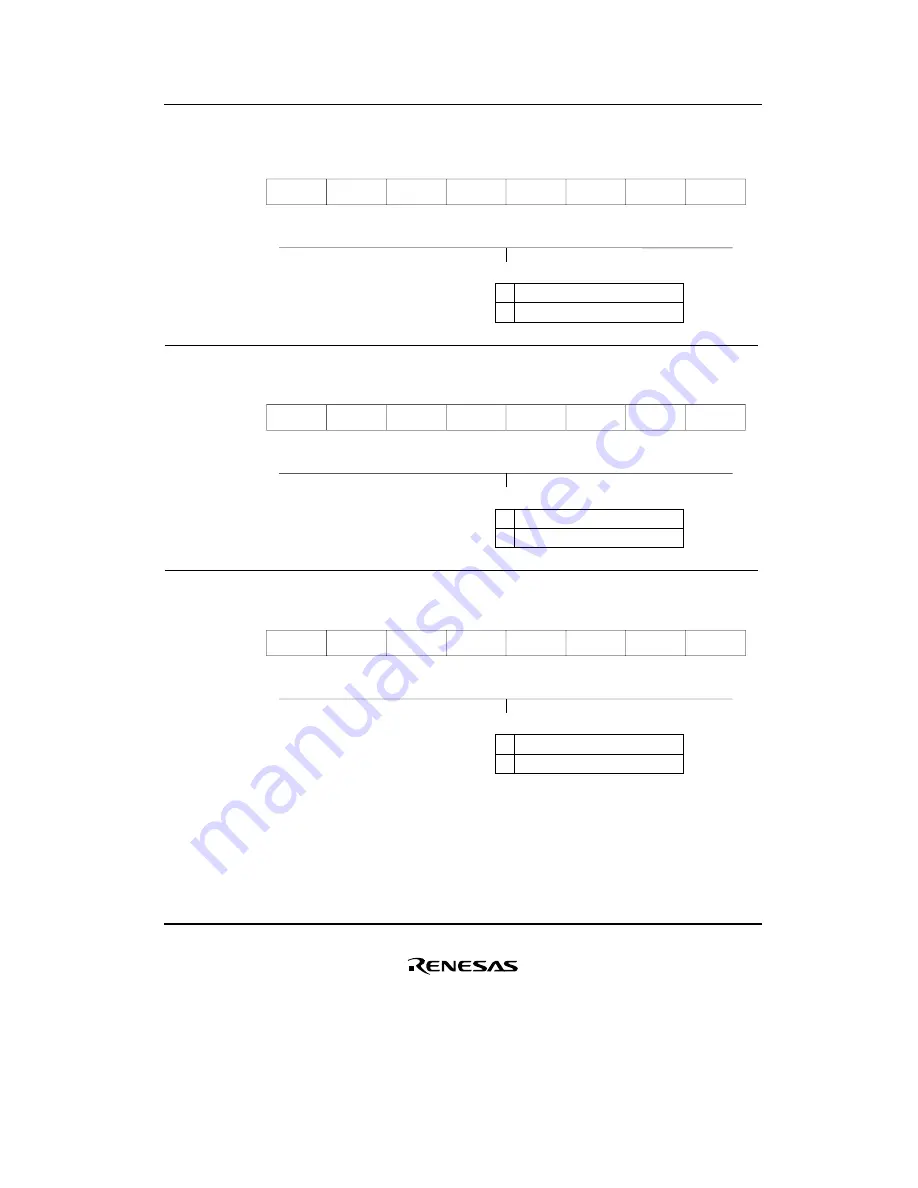
PCR1—Port control register 1


H'FFE4


I/O ports

Bit

Initial value

Read/Write

7

PCR1  

0

W

6

PCR1  

0

W

5

PCR1  

0

W

4

PCR1  

0

W

3

0

0

PCR1  

0

W

2

0

1

0

Port 1 input/output select

0

Input pin

1

Output pin

7

6

5

4

0


PCR2—Port control register 2


H'FFE5


I/O ports

Bit

Initial value

Read/Write

7

— 

0

6

—  

0

5

—  

0

4

—  

0

3

— 

0

0

PCR2  

0

W

2

PCR2  

0

W

1

PCR2  

0

W

Port 2 input/output select

0

Input pin

1

Output pin

0

2

1


PCR3—Port control register 3


H'FFE6


I/O ports

Bit

Initial value

Read/Write

7

0

6

0

5

0

4

0

3

0

0

PCR3  

0

W

2

PCR3  

0

W

1

PCR3  

0

W

Port 3 input/output select

0

Input pin

1

Output pin

0

2

1


Summary of Contents for F-ZTAT H8/3642A Series

Page 1: ...ook over all the business of both companies Therefore although the old company name remains in this document it is a valid Renesas Electronics document We appreciate your understanding Renesas Electronics website http www renesas com April 1st 2010 Renesas Electronics Corporation Issued by Renesas Electronics Corporation http www renesas com Send any inquiries to http www renesas com inquiry ...

Page 2: ...ct for an application categorized as Specific or for which the product is not intended where you have failed to obtain the prior written consent of Renesas Electronics The quality grade of each Renesas Electronics product is Standard unless otherwise expressly specified in a Renesas Electronics data sheets or data books etc Standard Computers office equipment communications equipment test and meas...

Page 3: ...R HD6473644R HD6433644 HD6433644R HD64F3644 H8 3643 HD6433643 H8 3643R HD6433643R HD64F3643 H8 3642 HD6433642 H8 3642R HD6433642R HD64F3642A H8 3641 HD6433641 H8 3641R HD6433641R H8 3640 HD6433640 H8 3640R HD6433640R The revision list can be viewed directly by clicking the title page The revision list summarizes the locations of revisions and additions Details should always be checked by referring...

Page 4: ... a total system before making a final decision on the applicability of the information and products Renesas Technology Corp assumes no responsibility for any damage liability or other loss resulting from the information contained herein 5 Renesas Technology Corp semiconductors are not designed or manufactured for use in a device or system that is used under circumstances in which human life is pot...

Page 5: ...ialization Note When power is first supplied the product s state is undefined The states of internal circuits are undefined until full power is supplied throughout the chip and a low level is input on the reset pin During the period where the states are undefined the register settings and the output state of each pin are also undefined Design your system so that it does not malfunction because of ...

Page 6: ...Rev 6 00 Sep 12 2006 page iv of xx ...

Page 7: ...with the H8 300 CPU The H8 3644 Group has a system on a chip architecture that includes such peripheral functions as a D A converter five timers a 14 bit PWM a two channel serial communication interface and an A D converter This makes it ideal for use in advanced control systems This manual describes the hardware of the H8 3644 Group For details on the H8 3644 Group instruction set refer to the H8...

Page 8: ...Rev 6 00 Sep 12 2006 page vi of xx ...

Page 9: ...ts the input sensing of the INT7 pin Bit 7 INTEG7 Description 0 Falling edge of INT7 pin input is detected initial value 1 Rising edge of INT7 pin input is detected 6 2 2 Memory Map Table 6 2 Socket Adapter Figure 6 2 Socket Adapter Pin Correspondence ZTAT 102 103 Description of socket adapter deleted 6 8 2 Memory Map Table 6 14 Socket Adapter Product Codes Figure 6 19 Socket Adapter Pin Correspon...

Page 10: ...ting operation status and error status 10 3 1 Overview Figure 10 6 SCI3 Block Diagram 291 Figure amended Clock TXD RXD SCK3 BRR SMR SCR3 SSR TDR RDR TSR RSR Transmit receive control circuit Internal data bus Interrupt request TEI TXI RXI ERI Internal clock φ 64 φ 16 φ 4 φ External clock BRC Baud rate generator 10 3 7 Interrupts Table 10 16 SCI3 Interrupt Requests 336 Table amended Vector Address H...

Page 11: ...nce value Sleep mode current dissipation ISLEEP1 VCC 5 7 mA Sleep high speed mode VCC 5 V fOSC 10 MHz 1 2 2 VCC 2 5 V fOSC 10 MHz 1 2 Reference value ISLEEP2 VCC 2 3 mA Sleep medium speed mode VCC 5 V fOSC 10 MHz 1 2 1 VCC 2 5 V fOSC 10 MHz 1 2 Reference value 13 2 5 AC Characteristics HD6433644 HD6433643 HD6433642 HD6433641 HD6433640 Table 13 9 Serial Interface SCI3 Timing 380 Table amended VCC 2...

Page 12: ...struction Length Bytes Operand Size xx 8 16 Rn Rn d 16 Rn Rn Rn aa 8 16 d 8 PC aa Implied No of States I H N Z V C Condition Code PUSH Rs ADD B xx 8 Rd SP 2 SP Rs16 SP Rd8 xx 8 Rd8 W B 2 0 6 2 2 B 2 Functions IEGR2 Interrupt edge select register 2 485 Bit table amended INT7 edge select 0 Falling edge of INT7 pin input is detected Rising edge of INT7 pin input is detected 1 ...

Page 13: ... Formats in General Registers 21 2 3 2 Memory Data Formats 22 2 4 Addressing Modes 23 2 4 1 Addressing Modes 23 2 4 2 Effective Address Calculation 25 2 5 Instruction Set 29 2 5 1 Data Transfer Instructions 31 2 5 2 Arithmetic Operations 33 2 5 3 Logic Operations 34 2 5 4 Shift Operations 34 2 5 5 Bit Manipulations 36 2 5 6 Branching Instructions 40 2 5 7 System Control Instructions 42 2 5 8 Block...

Page 14: ...al Interrupts 71 3 3 4 Internal Interrupts 72 3 3 5 Interrupt Operations 72 3 3 6 Interrupt Response Time 77 3 4 Application Notes 78 3 4 1 Notes on Stack Area Use 78 3 4 2 Notes on Rewriting Port Mode Registers 79 Section 4 Clock Pulse Generators 81 4 1 Overview 81 4 1 1 Block Diagram 81 4 1 2 System Clock and Subclock 81 4 2 System Clock Generator 82 4 3 Subclock Generator 84 4 4 Prescalers 85 4...

Page 15: ...Active Medium Speed Mode 99 5 7 2 Clearing Active Medium Speed Mode 99 5 7 3 Operating Frequency in Active Medium Speed Mode 99 5 8 Direct Transfer 100 Section 6 ROM 103 6 1 Overview 103 6 1 1 Block Diagram 103 6 2 PROM Mode 104 6 2 1 Setting to PROM Mode 104 6 2 2 Memory Map 104 6 3 Programming 105 6 3 1 Writing and Verifying 106 6 3 2 Programming Precautions 109 6 3 3 Reliability of Programmed D...

Page 16: ...mory PROM Mode H8 3644F H8 3643F and H8 3642AF 150 6 8 1 PROM Mode Setting 150 6 8 2 Memory Map 150 6 8 3 Operation in PROM Mode 151 6 9 Flash Memory Programming and Erasing Precautions 160 Section 7 RAM 167 7 1 Overview 167 7 1 1 Block Diagram 167 Section 8 I O Ports 169 8 1 Overview 169 8 2 Port 1 171 8 2 1 Overview 171 8 2 2 Register Configuration and Description 171 8 2 3 Pin Functions 175 8 2...

Page 17: ...ion 192 8 7 3 Pin Functions 194 8 7 4 Pin States 195 8 8 Port 8 195 8 8 1 Overview 195 8 8 2 Register Configuration and Description 196 8 8 3 Pin Functions 197 8 8 4 Pin States 198 8 9 Port 9 199 8 9 1 Overview 199 8 9 2 Register Configuration and Description 199 8 9 3 Pin Functions 200 8 9 4 Pin States 201 8 10 Port B 201 8 10 1 Overview 201 8 10 2 Register Configuration and Description 201 8 10 ...

Page 18: ...on 256 9 5 5 Timer X Operation Modes 263 9 5 6 Interrupt Sources 263 9 5 7 Timer X Application Example 264 9 5 8 Application Notes 265 9 6 Watchdog Timer 270 9 6 1 Overview 270 9 6 2 Register Descriptions 271 9 6 3 Timer Operation 274 9 6 4 Watchdog Timer Operation States 275 Section 10 Serial Communication Interface 277 10 1 Overview 277 10 2 SCI1 277 10 2 1 Overview 277 10 2 2 Register Descripti...

Page 19: ... 3 Pin Configuration 347 12 1 4 Register Configuration 347 12 2 Register Descriptions 348 12 2 1 A D Result Register ADRR 348 12 2 2 A D Mode Register AMR 348 12 2 3 A D Start Register ADSR 350 12 3 Operation 351 12 3 1 A D Conversion Operation 351 12 3 2 Start of A D Conversion by External Trigger Input 351 12 4 Interrupts 352 12 5 Typical Use 352 12 6 Application Notes 355 Section 13 Electrical ...

Page 20: ...upply Voltage and Operating Range 406 13 4 2 DC Characteristics HD64F3644 HD64F3643 HD64F3642A 409 13 4 3 AC Characteristics HD64F3644 HD64F3643 HD64F3642A 415 13 4 4 A D Converter Characteristics 419 13 5 Operation Timing 420 13 6 Output Load Circuit 423 Appendix A CPU Instruction Set 425 A 1 Instructions 425 A 2 Operation Code Map 433 A 3 Number of Execution States 435 Appendix B Internal I O Re...

Page 21: ...Rev 6 00 Sep 12 2006 page xix of xx Appendix E Product Code Lineup 522 Appendix F Package Dimensions 524 ...

Page 22: ...Rev 6 00 Sep 12 2006 page xx of xx ...

Page 23: ...Other on chip peripheral functions include five timers a 14 bit pulse width modulator PWM two serial communication interface channels and an A D converter providing an ideal configuration as a microcomputer for embedding in high level control systems In addition to the mask ROM version the H8 3644 is also available in a ZTAT 1 version with on chip user programmable PROM and an F ZTAT 2 version wit...

Page 24: ... MHz 1 Can run on 32 768 kHz subclock Instruction set compatible with H8 300 CPU Instruction length of 2 bytes or 4 bytes Basic arithmetic operations between registers MOV instruction for data transfer between memory and registers Typical instructions Multiply 8 bits 8 bits Divide 16 bits 8 bits Bit accumulator Register indirect designation of bit position Interrupts 33 interrupt sources 12 extern...

Page 25: ...H8 3641 12 kbyte ROM 512 byte RAM H8 3640 8 kbyte ROM 512 byte RAM I O ports 53 pins 45 I O pins 8 input pins Timers Five on chip timers Timer A 8 bit timer Count up timer with selection of eight internal clock signals divided from the system clock φ 2 and four clock signals divided from the watch clock φ w 2 Timer B1 8 bit timer Count up timer with selection of seven internal clock signals or eve...

Page 26: ...erial communication interface Two on chip serial communication interface channels SCI1 synchronous serial interface Choice of 8 bit or 16 bit data transfer SCI3 8 bit synchronous asynchronous serial interface Incorporates multiprocessor communication function 14 bit PWM Pulse division PWM output for reduced ripple Can be used as a 14 bit D A converter by connecting to an external low pass filter A...

Page 27: ... 64 pin SDIP DP 64S HD6433643W HD6433643RW HD64F3643W 80 pin TQFP TFP 80C HD6433642H HD6433642RH HD64F3642AH 64 pin QFP FP 64A ROM 16 kbytes RAM 512 kbytes HD6433642P HD6433642RP HD64F3642AP 64 pin SDIP DP 64S RAM 1 kbyte F ZTAT version HD6433642W HD6433642RW HD64F3642AW 80 pin TQFP TFP 80C HD6433641H HD6433641RH 64 pin QFP FP 64A ROM 12 kbytes RAM 512 bytes HD6433641P HD6433641RP 64 pin SDIP DP 6...

Page 28: ...53 INT3 P52 INT2 P51 INT1 P50 INT0 Port 1 P10 TMOW P14 PWM P15 IRQ1 P16 IRQ2 P17 IRQ3 TRGV Port 2 P20 SCK3 P21 RXD P22 TXD Port 3 P30 SCK1 P31 SI1 P32 SO1 P90 FVPP P91 P92 P93 P94 Port 9 PB 0 AN 0 PB 1 AN 1 PB 2 AN 2 PB 3 AN 3 PB 4 AN 4 PB 5 AN 5 PB 6 AN 6 PB 7 AN 7 V SS V CC RES IRQ 0 TEST OSC 1 OSC 2 X 1 X 2 CPU H8 300L Data bus lower System clock generator Subclock generator RAM Timer A SCI1 Ti...

Page 29: ... INT4 P53 INT3 P52 INT2 P51 INT1 P50 INT0 P67 P66 P65 P64 P63 P62 P61 P60 32 31 30 29 28 27 26 25 24 23 22 21 20 19 18 17 P2 1 RXD P2 0 SCK 3 P8 7 P8 6 FTID P8 5 FTIC P8 4 FTIB P8 3 FTIA P8 2 FTOB P8 1 FTOA P8 0 FTCI P7 7 P7 6 TMOV P7 5 TMCIV P7 4 TMRIV P7 3 V CC PB 1 AN 1 PB 0 AN 0 AV SS TEST X 2 X 1 V SS OSC 1 OSC 2 RES P9 0 FV PP P9 1 P9 2 P9 3 P9 4 IRQ 0 P22 TXD P32 SO1 P31 SI1 P30 SCK1 P10 TM...

Page 30: ...1 P32 SO1 P22 TXD P21 RXD P20 SCK3 P87 P86 FTID P85 FTIC P84 FTIB P83 FTIA P82 FTOB P81 FTOA P80 FTCI P77 P76 TMOV P75 TMCIV P74 TMRIV P73 VCC P57 INT7 P56 INT6 TMIB P55 INT5 ADTRG P54 INT4 P53 INT3 P52 INT2 P51 INT1 P50 INT0 P17 IRQ3 TRGV AVCC PB7 AN7 PB6 AN6 PB5 AN5 PB4 AN4 PB3 AN3 PB2 AN2 PB1 AN1 PB0 AN0 AVSS TEST X2 X1 VSS OSC1 OSC2 RES P90 FVPP P91 P92 P93 P94 IRQ0 P60 P61 P62 P63 P64 P65 P66...

Page 31: ...RIV P7 3 V CC NC 60 59 58 57 56 55 54 53 52 51 50 49 48 47 46 45 44 43 42 41 NC NC P22 TXD P32 SO1 P31 SI1 P30 SCK1 P10 TMOW P14 PWM P15 IRQ1 P16 IRQ2 P17 IRQ3 TRGV AVCC PB7 AN7 PB6 AN6 PB5 AN5 PB4 AN4 PB3 AN3 PB2 AN2 NC NC NC NC P57 INT7 P56 INT6 TMIB P55 INT5 ADTRG P54 INT4 P53 INT3 P52 INT2 P51 INT1 P50 INT0 NC P67 P66 P65 P64 P63 P62 P61 P60 NC 61 62 63 64 65 66 67 68 69 70 71 72 73 74 75 76 7...

Page 32: ...t used connect this pin to the user system VCC AVSS 3 11 4 Input Analog ground This is the A D converter ground pin It should be connected to the user system GND Clock pins OSC1 8 16 9 Input System clock These pins connect to a crystal or ceramic resonator or can be used to input an external clock OSC2 9 17 10 Output See section 4 Clock Pulse Generators for a typical connection diagram X1 6 14 7 I...

Page 33: ... 37 Input Timer B1 event counter input This is an event input pin for input to the timer B1 counter TMOV 37 45 46 Output Timer V output This is an output pin for waveforms generated by the timer V output compare function TMCIV 36 44 45 Input Timer V event input This is an event input pin for input to the timer V counter TMRIV 35 43 44 Input Timer V counter reset This is a counter reset input pin f...

Page 34: ... 64 1 2 3 to 10 73 to 78 2 3 Input Port B This is an 8 bit input port P17 to P14 P10 57 to 53 1 64 to 61 71 to 67 I O Port 1 This is a 5 bit I O port Input or output can be designated for each bit by means of port control register 1 PCR1 P22 to P20 49 to 47 57 to 55 63 59 58 I O Port 2 This is a 3 bit I O port Input or output can be designated for each bit by means of port control register 2 PCR2 ...

Page 35: ...ster 9 PCR9 Note There is no P90 function in the flash memory version since P90 is used as the FVPP pin Serial com munication SI1 51 59 65 Input SCI1 receive data input This is the SCI1 data input pin interface SCI SO1 50 58 64 Output SCI1 transmit data output This is the SCI1 data output pin SCK1 52 60 66 I O SCI1 clock I O This is the SCI1 clock I O pin RXD 48 56 59 Input SCI3 receive data input...

Page 36: ...ut On board programmable flash memory power supply Connected to the flash memory programming power supply 12 V When the flash memory is not being programmed connect to the user system VCC In versions other than the on chip flash memory version this pin is P90 Other NC 1 16 20 21 30 39 40 41 48 53 60 to 62 79 80 Non connected pins These pins must be left unconnected ...

Page 37: ...l bit manipulation instructions Eight addressing modes Register direct Register indirect Register indirect with displacement Register indirect with post increment or pre decrement Absolute address Immediate Program counter relative Memory indirect 64 kbyte address space High speed operation All frequently used instructions are executed in two to four states High speed arithmetic and logic operatio...

Page 38: ...tion 2 1 2 Address Space The H8 300L CPU supports an address space of up to 64 kbytes for storing program code and data See section 2 8 Memory Map for details of the memory map 2 1 3 Register Configuration Figure 2 1 shows the register structure of the H8 300L CPU There are two groups of registers the general registers and control registers ...

Page 39: ...H R7H R0L R1L R2L R3L R4L R5L R6L R7L SP SP Stack pointer PC Program counter CCR Condition code register Carry flag Overflow flag Zero flag Negative flag Half carry flag Interrupt mask bit User bit User bit CCR I U H U N Z V C General registers Rn Control registers CR 7 5 3 2 1 0 6 4 Figure 2 1 CPU Registers ...

Page 40: ...lso functions as the stack pointer SP used implicitly by hardware in exception processing and subroutine calls When it functions as the stack pointer as indicated in figure 2 2 SP R7 points to the top of the stack Lower address side H 0000 Upper address side H FFFF Unused area Stack area SP R7 Figure 2 2 Stack Pointer 2 2 2 Control Registers The CPU control registers include a 16 bit program count...

Page 41: ... B or NEG B instruction is executed this flag is set to 1 if there is a carry or borrow at bit 3 and is cleared to 0 otherwise The H flag is used implicitly by the DAA and DAS instructions When the ADD W SUB W or CMP W instruction is executed the H flag is set to 1 if there is a carry or borrow at bit 11 and is cleared to 0 otherwise Bit 4 User Bit U Can be used freely by the user Bit 3VNegative F...

Page 42: ...zed by software by the first instruction executed after a reset 2 3 Data Formats The H8 300L CPU can process 1 bit data 4 bit BCD data 8 bit byte data and 16 bit word data The H8 300L CPU can process 1 bit 4 bit BCD 8 bit byte and 16 bit word data 1 bit data is handled by bit manipulation instructions and is accessed by being specified as bit n n 0 1 2 7 in the operand data byte Byte data is handl...

Page 43: ... 0 1 bit data RnH 7 6 5 4 3 2 1 0 don t care 7 0 1 bit data RnL MSB LSB don t care 7 0 Byte data RnH Byte data RnL Word data Rn 4 bit BCD data RnH 4 bit BCD data RnL Legend RnH RnL MSB LSB Upper byte of general register Lower byte of general register Most significant bit Least significant bit MSB LSB don t care 7 0 MSB LSB 15 0 Upper digit Lower digit don t care 7 0 3 4 don t care Upper digit Lowe...

Page 44: ...ruction codes Data Format 7 6 5 4 3 2 1 0 Address Data Type 7 0 Address n MSB LSB MSB LSB Upper 8 bits Lower 8 bits MSB LSB CCR CCR MSB LSB MSB LSB Address n Even address Odd address Even address Odd address Even address Odd address 1 bit data Byte data Word data Byte data CCR on stack Word data on stack Legend CCR Condition code register Note Ignored on return Figure 2 4 Memory Data Formats When ...

Page 45: ...ave 16 bit operands 2 Register Indirect Rn The register field of the instruction specifies a 16 bit general register containing the address of the operand in memory 3 Register Indirect with Displacement d 16 Rn The instruction has a second word bytes 3 and 4 containing a displacement which is added to the contents of the specified general register to obtain the operand address in memory This mode ...

Page 46: ...ipulation instructions contain 3 bit immediate data in the second or fourth byte of the instruction specifying a bit number 7 Program Counter Relative d 8 PC This mode is used in the Bcc and BSR instructions An 8 bit displacement in byte 2 of the instruction code is sign extended to 16 bits and added to the program counter contents to generate a branch destination address and the PC contents to be...

Page 47: ...D OR and XOR instructions can also use immediate addressing 6 Data transfer instructions can use all addressing modes except program counter relative 7 and memory indirect 8 Bit manipulation instructions use register direct 1 register indirect 2 or 8 bit absolute addressing 5 to specify a byte operand and 3 bit immediate addressing 6 to specify a bit position in that byte The BSET BCLR BNOT and BT...

Page 48: ... 0 15 Register indirect Rn Contents 16 bits of register indicated by rm 0 15 0 15 3 Register indirect with displacement d 16 Rn op rm 7 6 3 4 0 15 disp 0 15 disp 0 15 Contents 16 bits of register indicated by rm 4 op rm 7 6 3 4 0 15 Register indirect with post increment Rn op rm 7 6 3 4 0 15 Register indirect with pre decrement Rn Incremented or decremented by 1 if operand is byte size and by 2 if...

Page 49: ...ective Address Calculation Method Effective Address EA 5 Absolute address aa 8 aa 16 op 8 7 0 15 0 15 abs H FF 8 7 0 15 0 15 abs op 6 op 0 15 IMM xx 16 op 8 7 0 15 IMM Immediate xx 8 Operand is 1 or 2 byte immediate data 7 op disp 7 0 15 Program counter relative d 8 PC PC contents 0 15 0 15 8 Sign extension disp ...

Page 50: ...ng Mode and Instruction Format Effective Address Calculation Method Effective Address EA 8 Memory indirect aa 8 op 8 7 0 15 Memory contents 16 bits 0 15 abs H 00 8 7 0 15 abs Legend rm rn Register field op Operation field disp Displacement IMM Immediate data abs Absolute address ...

Page 51: ... NEG 14 Logic operations AND OR XOR NOT 4 Shift SHAL SHAR SHLL SHLR ROTL ROTR ROTXL ROTXR 8 Bit manipulation BSET BCLR BNOT BTST BAND BIAND BOR BIOR BXOR BIXOR BLD BILD BST BIST 14 Branch Bcc 2 JMP BSR JSR RTS 5 System control RTE SLEEP LDC STC ANDC ORC XORC NOP 8 Block data transfer EEPMOV 1 Total 55 Notes 1 PUSH Rn is equivalent to MOV W Rn SP POP Rn is equivalent to MOV W SP Rn 2 Bcc is a condi...

Page 52: ...dition code register N N negative flag of CCR Z Z zero flag of CCR V V overflow flag of CCR C C carry flag of CCR PC Program counter SP Stack pointer IMM Immediate data disp Displacement Addition Subtraction Multiplication Division AND logical OR logical Exclusive OR logical Move Logical negation logical complement 3 3 bit length 8 8 bit length 16 16 bit length Contents of operand indicated by eff...

Page 53: ...er and memory or moves immediate data to a general register The Rn Rn d 16 Rn aa 16 xx 16 Rn and Rn addressing modes are available for word data The aa 8 addressing mode is available for byte data only The R7 and R7 modes require a word size specification POP W SP Rn Pops a general register from the stack Equivalent to MOV W SP Rn PUSH W Rn SP Pushes general register onto the stack Equivalent to M...

Page 54: ... Rn disp 15 0 8 7 op rm rn Rm Rn or Rn Rm 15 0 8 7 op rn abs aa 8 Rn 15 0 8 7 op rn aa 16 Rn abs 15 0 8 7 op rn IMM xx 8 Rn 15 0 8 7 op rn xx 16 Rn IMM 15 0 8 7 op rn PUSH POP Legend op rm rn disp abs IMM Operation field Register field Displacement Absolute address Immediate data SP Rn or Rn SP 1 1 1 Figure 2 5 Data Transfer Instruction Codes ...

Page 55: ...ister INC DEC B Rd 1 Rd Increments or decrements a general register ADDS SUBS W Rd 1 Rd Rd 2 Rd Adds or subtracts 1 or 2 to or from a general register DAA DAS B Rd decimal adjust Rd Decimal adjusts adjusts to packed BCD an addition or subtraction result in a general register by referring to the CCR MULXU B Rd Rs Rd Performs 8 bit 8 bit unsigned multiplication on data in two general registers provi...

Page 56: ...orms a logical exclusive OR operation on a general register and another general register or immediate data NOT B Rd Rd Obtains the one s complement logical complement of general register contents Notes Size Operand size B Byte 2 5 4 Shift Operations Table 2 7 describes the eight shift instructions Table 2 7 Shift Instructions Instruction Size Function SHAL SHAR B Rd shift Rd Performs an arithmetic...

Page 57: ...MP ADDX SUBX Rm Legend op rm rn IMM Operation field Register field Immediate data 15 0 8 7 op rn ADDS SUBS INC DEC DAA DAS NEG NOT 15 0 8 7 op rn MULXU DIVXU rm 15 0 8 7 rn IMM ADD ADDX SUBX CMP XX 8 op 15 0 8 7 op rn AND OR XOR Rm rm 15 0 8 7 rn IMM AND OR XOR xx 8 op 15 0 8 7 rn SHAL SHAR SHLL SHLR ROTL ROTR ROTXL ROTXR op Figure 2 6 Arithmetic Logic and Shift Instruction Codes ...

Page 58: ... data or the lower three bits of a general register BTST B bit No of EAd Z Tests a specified bit in a general register or memory and sets or clears the Z flag accordingly The bit number is specified by 3 bit immediate data or the lower three bits of a general register BAND B C bit No of EAd C ANDs the C flag with a specified bit in a general register or memory and stores the result in the C flag B...

Page 59: ... No of EAd C Copies a specified bit in a general register or memory to the C flag BILD B bit No of EAd C Copies the inverse of a specified bit in a general register or memory to the C flag The bit number is specified by 3 bit immediate data BST B C bit No of EAd Copies the C flag to a specified bit in a general register or memory BIST B C bit No of EAd Copies the inverse of the C flag to a specifi...

Page 60: ...xx 3 rn 0 0 0 0 0 0 0 IMM 15 0 8 7 op 0 Operand Bit No register indirect Rn register direct Rm rn 0 0 0 0 0 0 0 rm op 15 0 8 7 op Operand Bit No absolute aa 8 immediate xx 3 abs 0 0 0 0 IMM op op 15 0 8 7 op Operand Bit No absolute aa 8 register direct Rm abs 0 0 0 0 rm op 15 0 8 7 op IMM rn Operand Bit No register direct Rn immediate xx 3 BAND BOR BXOR BLD BST 15 0 8 7 op 0 Operand Bit No registe...

Page 61: ...address Immediate data 15 0 8 7 op IMM rn Operand Bit No register direct Rn immediate xx 3 BIAND BIOR BIXOR BILD BIST 15 0 8 7 op 0 Operand Bit No register indirect Rn immediate xx 3 rn 0 0 0 0 0 0 0 IMM op 15 0 8 7 op Operand Bit No absolute aa 8 immediate xx 3 abs 0 0 0 0 IMM op Figure 2 7 Bit Manipulation Instruction Codes cont ...

Page 62: ...Description Condition BRA BT Always true Always BRN BF Never false Never BHI High C Z 0 BLS Low or same C Z 1 BCC BHS Carry clear high or same C 0 BCS BLO Carry set low C 1 BNE Not equal Z 0 BEQ Equal Z 1 BVC Overflow clear V 0 BVS Overflow set V 1 BPL Plus N 0 BMI Minus N 1 BGE Greater or equal N V 0 BLT Less than N V 1 BGT Greater than Z N V 0 BLE Less or equal Z N V 1 JMP Branches unconditional...

Page 63: ...on field Register field Displacement Absolute address 15 0 8 7 op cc disp Bcc 15 0 8 7 op rm 0 JMP Rm 0 0 0 15 0 8 7 op JMP aa 16 abs 15 0 8 7 op abs JMP aa 8 15 0 8 7 op disp BSR 15 0 8 7 op rm 0 JSR Rm 0 0 0 15 0 8 7 op JSR aa 16 abs 15 0 8 7 op abs JSR aa 8 15 0 8 7 op RTS Figure 2 8 Branching Instruction Codes ...

Page 64: ...own mode See section 5 Power Down Modes for details LDC B Rs CCR IMM CCR Moves immediate data or general register contents to the condition code register STC B CCR Rd Copies the condition code register to a specified general register ANDC B CCR IMM CCR Logically ANDs the condition code register with immediate data ORC B CCR IMM CCR Logically ORs the condition code register with immediate data XORC...

Page 65: ...ction Figure 2 10 shows its object code format Table 2 11 Block Data Transfer Instruction Instruction Size Function EEPMOV If R4L 0 then repeat R5 R6 R4L 1 R4L until R4L 0 else next Block transfer instruction Transfers the number of data bytes specified by R4L from locations starting at the address indicated by R5 to locations starting at the address indicated by R6 After the transfer the next ins...

Page 66: ...d one state A bus cycle consists of two states or three states The cycle differs depending on whether access is to on chip memory or to on chip peripheral modules 2 6 1 Access to On Chip Memory RAM ROM Access to on chip memory takes place in two states The data bus width is 16 bits allowing access in byte or word size Figure 2 11 shows the on chip memory access cycle T1 state Bus cycle T2 state In...

Page 67: ... accessing word data two instructions must be used Two State Access to On Chip Peripheral Modules Figure 2 12 shows the operation timing in the case of two state access to an on chip peripheral module T1 state Bus cycle T2 state φ or φ Internal address bus Internal read signal Internal data bus read access Internal write signal Read data Address Write data Internal data bus write access SUB Figure...

Page 68: ...ata bus write access T2 state T3 state Write data SUB φ or φ Figure 2 13 On Chip Peripheral Module Access Cycle 3 State Access 2 7 CPU States 2 7 1 Overview There are four CPU states the reset state program execution state program halt state and exception handling state The program execution state includes active high speed or medium speed mode and subactive mode In the program halt state there ar...

Page 69: ...nchronized by the system clock The CPU executes successive program instructions at reduced speed synchronized by the system clock The CPU executes successive program instructions at reduced speed synchronized by the subclock A state in which some or all of the chip functions are stopped to conserve power A transient state in which the CPU changes the processing flow due to a reset or an interrupt ...

Page 70: ...chronized with the system clock in active mode high speed and medium speed and with the subclock in subactive mode See section 5 Power Down Modes for details on these modes 2 7 3 Program Halt State In the program halt state there are five modes two sleep modes high speed and medium speed standby mode watch mode and subsleep mode See section 5 Power Down Modes for details on these modes 2 7 4 Excep...

Page 71: ...On chip RAM Reserved Internal I O registers 16 bytes Internal I O registers 128 bytes H 0000 H 002F H 0030 H 1FFF H 3FFF H 5FFF H 7FFF H F770 H F77F H FB80 H FF9F H FFA0 H FFFF H 2FFF 8 kbytes H8 3640 H FF7F H FF80 H FF7F H FF80 12 kbytes H8 3641 12 kbytes H8 3642 24 kbytes H8 3643 32 kbytes H8 3644 512 bytes 512 bytes 512 bytes 1 kbyte 1 kbyte Figure 2 16 H8 3644 Group Memory Map ...

Page 72: ... Access to internal I O registers Internal data transfer to or from on chip modules other than the ROM and RAM areas makes use of an 8 bit data width If word access is attempted to these areas the following results will occur Word access from CPU to I O register area Upper byte Will be written to I O register Lower byte Transferred data will be lost Word access from I O register to CPU Upper byte ...

Page 73: ...H 002F H 0030 H 7FFF H F770 H F77F H FB80 H FF7F H FF80 H FF9F H FFA0 H FFFF Word Byte Access States 2 or 3 2 3 2 Reserved Reserved Notes The H8 3644 is shown as an example Internal I O registers in areas assigned to timer X H F770 to H F77F SCI3 H FFA8 to H FFAD and timer V H FFB8 to H FFBD are accessed in three states Figure 2 17 Data Size and Number of States for Access to and from On Chip Peri...

Page 74: ... 1 timer load register and timer counter Figure 2 18 shows an example in which two timer registers share the same address When a bit manipulation instruction accesses the timer load register and timer counter of a reloadable timer since these two registers share the same address the following operations take place Order of Operation Operation 1 Read Timer counter data is read one byte 2 Modify The...

Page 75: ... 0 0 0 B BSET instruction executed BSET 0 PDR3 The BSET instruction is executed designating port 3 C After executing BSET P37 P36 P35 P34 P33 P32 P31 P30 Input output Input Input Output Output Output Output Output Output Pin state Low level High level Low level Low level Low level Low level Low level High level PCR3 0 0 1 1 1 1 1 1 PDR3 0 1 0 0 0 0 0 1 D Explanation of how BSET operates When the B...

Page 76: ...to PDR3 P37 P36 P35 P34 P33 P32 P31 P30 Input output Input Input Output Output Output Output Output Output Pin state Low level High level Low level Low level Low level Low level Low level Low level PCR3 0 0 1 1 1 1 1 1 PDR3 1 0 0 0 0 0 0 0 RAM0 1 0 0 0 0 0 0 0 B BSET instruction executed BSET 0 RAM0 The BSET instruction is executed designating the PDR3 work area RAM0 C After executing BSET MOV B R...

Page 77: ...put Output Output Pin state Low level High level Low level Low level Low level Low level Low level Low level PCR3 0 0 1 1 1 1 1 1 PDR3 1 0 0 0 0 0 0 0 B BCLR instruction executed BCLR 0 PCR3 The BCLR instruction is executed designating PCR3 C After executing BCLR P37 P36 P35 P34 P33 P32 P31 P30 Input output Output Output Output Output Output Output Output Input Pin state Low level High level Low l...

Page 78: ...AM0 as well as to PCR3 P37 P36 P35 P34 P33 P32 P31 P30 Input output Input Input Output Output Output Output Output Output Pin state Low level High level Low level Low level Low level Low level Low level Low level PCR3 0 0 1 1 1 1 1 1 PDR3 1 0 0 0 0 0 0 0 RAM0 0 0 1 1 1 1 1 1 B BCLR instruction executed BCLR 0 RAM0 The BCLR instruction is executed designating the PCR3 work area RAM0 C After executi...

Page 79: ... data register 2 PDR2 H FFD5 Port data register 3 PDR3 H FFD6 Port data register 5 PDR5 H FFD8 Port data register 6 PDR6 H FFD9 Port data register 7 PDR7 H FFDA Port data register 8 PDR8 H FFDB Port data register 9 PDR9 H FFDC Note Port data registers have the same addresses as input pins Table 2 13 Registers with Write Only Bits Register Name Abbreviation Address Port control register 1 PCR1 H FF...

Page 80: ...ruction It moves the number of bytes specified by R4L from the address specified by R5 to the address specified by R6 R6 R6 R4L R5 R5 R4L When setting R4L and R6 make sure that the final destination address R6 R4L does not exceed H FFFF The value in R6 must not change from H FFFF to H 0000 during execution of the instruction H FFFF Not allowed R6 R6 R4L R5 R5 R4L ...

Page 81: ...xecution of the present instruction or the exception handling in progress is completed 3 2 Reset 3 2 1 Overview A reset is the highest priority exception The internal state of the CPU and the registers of the on chip peripheral modules are initialized 3 2 2 Reset Sequence Reset by RES RES RES RES Pin As soon as the RES pin goes low all processing is stopped and the chip enters the reset state To m...

Page 82: ...ss H 0000 to H 0001 after which the program starts executing from the address indicated in PC When system power is turned on or off the RES pin should be held low Figure 3 1 shows the reset sequence starting from RES input Vector fetch φ Internal address bus Internal read signal Internal write signal Internal data bus 16 bit RES Internal processing Program initial instruction prefetch 1 Reset exce...

Page 83: ... the stack correctly resulting in program runaway To prevent this immediately after reset exception handling all interrupts are masked For this reason the initial program instruction is always executed immediately after a reset This instruction should initialize the stack pointer e g MOV W xx 16 SP 3 3 Interrupts 3 3 1 Overview The interrupt sources include 12 external interrupts IRQ3 to IRQ0 INT7...

Page 84: ... 0017 Timer X Timer X input capture A 16 H 0020 to H 0021 Timer X input capture B Timer X input capture C Timer X input capture D Timer X compare match A Timer X compare match B Timer X overflow Timer V Timer V compare match A 17 H 0022 to H 0023 Timer V compare match B Timer V overflow SCI1 SCI1 transfer complete 19 H 0026 to H 0027 SCI3 SCI3 transmit end 21 H 002A to H 002B SCI3 transmit data em...

Page 85: ...FFF8 Interrupt request register 3 IRR3 R W H 00 H FFF9 Note Write is enabled only for writing of 0 to clear a flag Interrupt Edge Select Register 1 IEGR1 Bit 7 6 5 4 3 2 1 0 IEG3 IEG2 IEG1 IEG0 Initial value 0 1 1 1 0 0 0 0 Read Write R W R W R W R W IEGR1 is an 8 bit read write register used to designate whether pins IRQ3 to IRQ0 are set to rising edge sensing or falling edge sensing Upon reset I...

Page 86: ...ut sensing of pin IRQ0 Bit 0 IEG0 Description 0 Falling edge of IRQ0 pin input is detected initial value 1 Rising edge of IRQ0 pin input is detected Interrupt Edge Select Register 2 IEGR2 Bit 7 6 5 4 3 2 1 0 INTEG7 INTEG6 INTEG5 INTEG4 INTEG3 INTEG2 INTEG1 INTEG0 Initial value 0 0 0 0 0 0 0 0 Read Write R W R W R W R W R W R W R W R W IEGR2 is an 8 bit read write register used to designate whether...

Page 87: ... detected Bits 4 to 0 INT4 to INT0 Edge Select INTEG4 to INTEG0 Bits 4 to 0 select the input sensing of pins INT4 to INT0 Bit n INTEGn Description 0 Falling edge of INTn pin input is detected initial value 1 Rising edge of INTn pin input is detected n 4 to 0 Interrupt Enable Register 1 IENR1 Bit 7 6 5 4 3 2 1 0 IENTB1 IENTA IEN3 IEN2 IEN1 IEN0 Initial value 0 0 0 1 0 0 0 0 Read Write R W R W R W R...

Page 88: ...Enable IEN3 to IEN0 Bits 3 to 0 enable or disable IRQ3 to IRQ0 interrupt requests Bit n IENn Description 0 Disables interrupt requests from pin IRQn initial value 1 Enables interrupt requests from pin IRQn n 3 to 0 Interrupt Enable Register 2 IENR2 Bit 7 6 5 4 3 2 1 0 IENDT IENAD IENS1 Initial value 0 0 0 0 0 0 0 0 Read Write R W R W R W IENR2 is an 8 bit read write register that enables or disabl...

Page 89: ...errupt requests initial value 1 Enables SCI1 interrupt requests Bits 3 to 0 Reserved Bits Bits 3 to 0 are reserved they are always read as 0 and cannot be modified Interrupt Enable Register 3 IENR3 Bit 7 6 5 4 3 2 1 0 INTEN7 INTEN6 INTEN5 INTEN4 INTEN3 INTEN2 INTEN1 INTEN0 Initial value 0 0 0 0 0 0 0 0 Read Write R W R W R W R W R W R W R W R W IENR3 is an 8 bit read write register that enables or...

Page 90: ...ed It is necessary to write 0 to clear each flag Upon reset IRR1 is initialized to H 10 Bit 7 Timer B1 Interrupt Request Flag IRRTB1 Bit 7 IRRTB1 Description 0 Clearing condition initial value When IRRTB1 1 it is cleared by writing 0 1 Setting condition When the timer B1 counter value overflows from H FF to H 00 Bit 6 Timer A Interrupt Request Flag IRRTA Bit 6 IRRTA Description 0 Clearing conditio...

Page 91: ...e register in which a corresponding flag is set to 1 when a direct transfer A D converter or SCI1 interrupt is requested The flags are not cleared automatically when an interrupt is accepted It is necessary to write 0 to clear each flag Upon reset IRR2 is initialized to H 00 Bit 7 Direct Transfer Interrupt Request Flag IRRDT Bit 7 IRRDT Description 0 Clearing condition initial value When IRRDT 1 i...

Page 92: ... 5 4 3 2 1 0 INTF7 INTF6 INTF5 INTF4 INTF3 INTF2 INTF1 INTF0 Initial value 0 0 0 0 0 0 0 0 Read Write R W R W R W R W R W R W R W R W Note Only a write of 0 for flag clearing is possible IRR3 is an 8 bit read write register in which a corresponding flag is set to 1 by a transition at pin INT7 to INT0 The flags are not cleared automatically when an interrupt is accepted It is necessary to write 0 t...

Page 93: ...o 4 are assigned to interrupts IRQ3 to IRQ0 The order of priority is from IRQ0 high to IRQ3 low Table 3 2 gives details INT Interrupts INT interrupts are requested by input signals to pins INT7 to INT0 These interrupts are detected by either rising edge sensing or falling edge sensing depending on the settings of bits INTEG7 to INTEG0 in IEGR2 When the designated edge is input at pins INT7 to INT0...

Page 94: ...tting the I bit to 1 in CCR When internal interrupt handling is initiated the I bit is set to 1 in CCR Vector numbers from 23 to 9 are assigned to these interrupts Table 3 2 shows the order of priority of interrupts from on chip peripheral modules 3 3 5 Interrupt Operations Interrupts are controlled by an interrupt controller Figure 3 2 shows a block diagram of the interrupt controller Figure 3 3 ...

Page 95: ...is accepted after processing of the current instruction is completed both PC and CCR are pushed onto the stack The state of the stack at this time is shown in figure 3 4 The PC value pushed onto the stack is the address of the first instruction to be executed upon return from interrupt handling The I bit of CCR is set to 1 masking further interrupts The vector address corresponding to the accepted...

Page 96: ...s saved I 1 I 0 Program execution state No Yes Yes No Legend PC CCR I Program counter Condition code register I bit of CCR IEN0 1 No Yes IENDT 1 No Yes IRRDT 1 No Yes Branch to interrupt handling routine IRRI0 1 No Yes IEN1 1 No Yes IRRI1 1 No Yes IEN2 1 No Yes IRRI2 1 Figure 3 3 Flow up to Interrupt Acceptance ...

Page 97: ...ounter PC Lower 8 bits of program counter PC Condition code register Stack pointer Notes CCR CCR PCH PCL 1 2 PC shows the address of the first instruction to be executed upon return from the interrupt handling routine Register contents must always be saved and restored by word access starting from an even numbered address Figure 3 4 Stack State after Completion of Interrupt Exception Handling Figu...

Page 98: ...ss Instruction is not executed Address is saved as PC contents becoming return address 2 4 Instruction code not executed 3 Instruction prefetch address Instruction is not executed 5 SP 2 6 SP 4 7 CCR 8 Vector address 9 Starting address of interrupt handling routine contents of vector 10 First instruction of interrupt handling routine 3 9 8 6 5 4 1 7 10 Stack access Internal processing Instruction ...

Page 99: ...s after an interrupt request flag is set until the first instruction of the interrupt handler is executed Table 3 4 Interrupt Wait States Item States Waiting time for completion of executing instruction 1 to 13 Saving of PC and CCR to stack 4 Vector fetch 2 Instruction fetch 4 Internal processing 4 Total 15 to 27 Note Not including EEPMOV instruction ...

Page 100: ...a program to crash An example is shown in figure 3 6 PC PC R1L PC SP SP SP H FEFC H FEFD H FEFF H L L MOV B R1L R7 SP set to H FEFF Stack accessed beyond SP BSR instruction Contents of PC are lost H Legend PCH PCL R1L SP Upper byte of program counter Lower byte of program counter General register R1L Stack pointer Figure 3 6 Operation when Odd Address Is Set in SP When CCR contents are saved to th...

Page 101: ...and IEGR bit IEG3 1 IRRI2 When PMR1 bit IRQ2 is changed from 0 to 1 while pin IRQ2 is low and IEGR bit IEG2 0 When PMR1 bit IRQ2 is changed from 1 to 0 while pin IRQ2 is low and IEGR bit IEG2 1 IRRI1 When PMR1 bit IRQ1 is changed from 0 to 1 while pin IRQ1 is low and IEGR bit IEG1 0 When PMR1 bit IRQ1 is changed from 1 to 0 while pin IRQ1 is low and IEGR bit IEG1 1 Figure 3 7 shows the procedure f...

Page 102: ...her possibility is to disable the relevant interrupt in interrupt enable register 1 After setting the port mode register bit first execute at least one instruction e g NOP then clear the interrupt request flag to 0 Interrupt mask cleared Clear interrupt request flag to 0 CCR I bit 0 Figure 3 7 Port Mode Register Setting and Interrupt Request Flag Clearing Procedure ...

Page 103: ...der 1 2 1 4 1 8 System clock divider 1 64 1 32 1 16 1 8 System clock pulse generator Subclock pulse generator Prescaler S 13 bits Prescaler W 5 bits OSC OSC 1 2 X X 1 2 φOSC f OSC φW f W φ 2 OSC φ 2 W φ 8 W φSUB φ 2 to φ 8192 φ 2 W φ 4 W φ 8 to φ 128 W W φ φOSC 128 φOSC 64 φOSC 32 φOSC 16 φ 4 W Figure 4 1 Block Diagram of Clock Pulse Generators 4 1 2 System Clock and Subclock The basic clock signa...

Page 104: ... shows a typical method of connecting a crystal resonator 1 2 C1 C2 OSC OSC R 1 M 20 C C 12 pF 20 f 1 2 Ω Rf Figure 4 2 Typical Connection to Crystal Resonator Figure 4 3 shows the equivalent circuit of a crystal resonator An oscillator having the characteristics given in table 4 1 should be used CS C0 RS OSC1 OSC2 LS Figure 4 3 Equivalent Circuit of Crystal Resonator Table 4 1 Crystal Resonator P...

Page 105: ...onator Notes on Board Design When generating clock pulses by connecting a crystal or ceramic resonator pay careful attention to the following points Avoid running signal lines close to the oscillator circuit since the oscillator may be adversely affected by induction currents See figure 4 5 The board should be designed so that the oscillator and load capacitors are located as close as possible to ...

Page 106: ...en Figure 4 6 External Clock Input Example Frequency Oscillator Clock φ φ φ φOSC Duty cycle 45 to 55 4 3 Subclock Generator Connecting a 32 768 kHz Crystal Resonator Clock pulses can be supplied to the subclock divider by connecting a 32 768 kHz crystal resonator as shown in figure 4 7 Follow the same precautions as noted under section 4 2 Notes on Board Design X X C1 C2 1 2 C C 15 pF typ 1 2 Figu...

Page 107: ...when not Using Subclock 4 4 Prescalers The H8 3644 Group is equipped with two on chip prescalers having different input clocks prescaler S and prescaler W Prescaler S is a 13 bit counter using the system clock φ as its input clock Its prescaled outputs provide internal clock signals for on chip peripheral modules Prescaler W is a 5 bit counter using a 32 768 kHz signal divided by 4 φW 4 as its inp...

Page 108: ...s counting on exit from the reset state Even in standby mode watch mode subactive mode or subsleep mode prescaler W continues functioning so long as clock signals are supplied to pins X1 and X2 Prescaler W can be reset by setting 1s in bits TMA3 and TMA2 of timer mode register A TMA Output from prescaler W can be used to drive timer A in which case timer A functions as a time base for timekeeping ...

Page 109: ...eripheral functions except PWM are operable on the system clock Sleep medium speed mode The CPU halts On chip peripheral functions except PWM are operable on the system clock but at 1 64 1 32 1 6 or 1 8 the speed in active high speed mode Subsleep mode The CPU halts The time base function of timer A are operable on the subclock Watch mode The CPU halts The time base function of timer A is operable...

Page 110: ... are given in the explanations of each mode in sections 5 2 through 5 8 Notes 1 2 Mode Transition Conditions 1 a b c d e f g h i J LSON MSON SSBY DTON 0 0 1 0 0 0 0 1 0 0 1 0 1 1 0 0 0 0 1 1 0 0 1 1 1 0 0 0 0 0 1 1 1 1 1 Don t care Mode Transition Conditions 2 1 Interrupt Sources Timer A interrupt IRQ0 interrupt Timer a interrupt IRQ3 to IRQ0 interrupts INT interrupt All interrupts IRQ1 or IRQ0 in...

Page 111: ...unctions Functions Functions Functions Functions Functions Functions Functions interrupts IRQ1 Retained 2 IRQ2 Retained 2 IRQ3 INT0 Functions Functions Functions Functions Retained 2 Functions Functions Retained 2 INT1 INT2 INT3 INT4 INT5 INT6 INT7 Peripheral Timer A Functions Functions Functions Functions Functions 3 Functions 3 Functions 3 Retained functions Timer B1 Retained Retained Retained T...

Page 112: ...e 0 0 0 0 0 1 1 1 Read Write R W R W R W R W R W R W R W SYSCR1 is an 8 bit read write register for control of the power down modes Upon reset SYSCR1 is initialized to H 07 Bit 7 Software Standby SSBY This bit designates transition to standby mode or watch mode Bit 7 SSBY Description 0 When a SLEEP instruction is executed in active mode a transition is made to sleep mode When a SLEEP instruction i...

Page 113: ...gend Don t care Bit 3 Low Speed on Flag LSON This bit chooses the system clock φ or subclock φSUB as the CPU operating clock when watch mode is cleared The resulting operation mode depends on the combination of other control bits and interrupt input Bit 3 LSON Description 0 The CPU operates on the system clock φ initial value 1 The CPU operates on the subclock φSUB Bits 2 Reserved Bits Bit 2 is re...

Page 114: ...itialized to H E0 Bits 7 to 5 Reserved Bits These bits are reserved they are always read as 1 and cannot be modified Bit 4 Noise Elimination Sampling Frequency Select NESEL This bit selects the frequency at which the watch clock signal φW generated by the subclock pulse generator is sampled in relation to the oscillator clock φOSC generated by the system clock pulse generator When φOSC 2 to 10 MHz...

Page 115: ... or to subactive mode if SSBY 1 TMA3 1 and LSON 1 When a SLEEP instruction is executed in active medium speed mode a direct transition is made to active high speed mode if SSBY 0 MSON 0 and LSON 0 or to subactive mode if SSBY 1 TMA3 1 and LSON 1 When a SLEEP instruction is executed in subactive mode a direct transition is made to active high speed mode if SSBY 1 TMA3 1 LSON 0 and MSON 0 or to acti...

Page 116: ...edium speed mode when a SLEEP instruction is executed while the SSBY and LSON bits in SYSCR1 are cleared to 0 the MSON bit in SYSCR2 is set to 1 and the DTON bit in SYSCR2 is cleared to 0 In sleep medium speed mode as in sleep high speed mode CPU operation is halted but the on chip peripheral functions other than PWM are operational The clock frequency in sleep medium speed mode is determined by t...

Page 117: ...imum RAM data retention voltage The I O ports go to the high impedance state 5 3 2 Clearing Standby Mode Standby mode is cleared by an interrupt IRQ1 or IRQ0 or by input at the RES pin Clearing by interrupt When an interrupt is requested the system clock pulse generator starts After the time set in bits STS2 STS0 in SYSCR1 has elapsed a stable system clock signal is supplied to the entire chip sta...

Page 118: ... states 6 6 8 2 16 4 32 8 65 5 0 1 1 65 536 states 13 1 16 4 32 8 65 5 131 1 1 131 072 states 26 2 32 8 65 5 131 1 262 1 Legend Don t care When an external clock is used Any values may be set Normally the minimum time STS2 STS1 STS0 0 should be set 5 4 Watch Mode 5 4 1 Transition to Watch Mode The system goes from active or subactive mode to watch mode when a SLEEP instruction is executed while th...

Page 119: ...tch mode is not cleared if the I bit of CCR is set to 1 or the particular interrupt is disabled in the interrupt enable register Clearing by RES input Clearing by RES pin is the same as for standby mode see section 5 3 2 Clearing Standby Mode 5 4 3 Oscillator Settling Time after Watch Mode Is Cleared The waiting time is the same as for standby mode see section 5 3 3 Oscillator Settling Time after ...

Page 120: ...ed while the LSON bit in SYSCR1 is set to 1 From subsleep mode subactive mode is entered if a timer A IRQ3 to IRQ0 or INT7 to INT0 interrupt is requested A transition to subactive mode does not take place if the I bit of CCR is set to 1 or the particular interrupt is disabled in the interrupt enable register 5 6 2 Clearing Subactive Mode Subactive mode is cleared by a SLEEP instruction or by input...

Page 121: ...instruction or by input at the RES pin Clearing by SLEEP instruction A transition to standby mode takes place if the SLEEP instruction is executed while the SSBY bit in SYSCR1 is set to 1 the LSON bit in SYSCR1 is cleared to 0 and the TMA3 bit in TMA is cleared to 0 The system goes to watch mode if the SSBY bit in SYSCR1 is set to 1 and bit TMA3 in TMA is set to 1 when a SLEEP instruction is execu...

Page 122: ...sfer from active medium speed mode to active high speed mode When a SLEEP instruction is executed in active medium speed mode while the SSBY and LSON bits in SYSCR1 are cleared to 0 the MSON bit in SYSCR2 is cleared to 0 and the DTON bit in SYSCR2 is set to 1 a transition is made to active high speed mode via sleep mode Direct transfer from active high speed mode to subactive mode When a SLEEP ins...

Page 123: ...ruction is executed in subactive mode while the SSBY bit in SYSCR1 is set to 1 the LSON bit in SYSCR1 is cleared to 0 the MSON bit in SYSCR2 is set to 1 the DTON bit in SYSCR2 is set to 1 and the TMA3 bit in TMA is set to 1 a transition is made directly to active medium speed mode via watch mode after the waiting time set in SYSCR1 bits STS2 to STS0 has elapsed ...

Page 124: ...Section 5 Power Down Modes Rev 6 00 Sep 12 2006 page 102 of 526 REJ09B0326 0600 ...

Page 125: ... speed two state access for both byte data and word data In the PROM version H8 3644 ZTAT and flash memory versions H8 3644 F ZTAT H8 3643 F ZTAT H8 3642 AF ZTAT programs can be written and erased with a general purpose PROM programmer In the on chip flash memory versions programs can be written and erased on board 6 1 1 Block Diagram Figure 6 1 shows a block diagram of the on chip ROM H 7FFE H 7F...

Page 126: ...ay as the standard HN27C256 EPROM Table 6 1 shows how to set the chip to PROM mode Table 6 1 Setting to PROM Mode Pin Name Setting TEST High level PB4 AN4 Low level PB5 AN5 PB6 AN6 High level 6 2 2 Memory Map Figure 6 2 shows a memory map On chip PROM H 0000 H 7FFF H 0000 H 7FFF Address in MCU mode Address in PROM mode Figure 6 2 H8 3644 Memory Map in PROM Mode When programming with a PROM program...

Page 127: ...on in PROM Mode H8 3644 Pin Mode CE CE CE CE OE OE OE OE VPP VCC EO7 to EO0 EA14 to EA0 Write L H VPP VCC Data input Address input Verify H L VPP VCC Data output Address input Programming disabled H H VPP VCC High impedance Address input Legend L Low level H High level VPP VPP level VCC VCC level The specifications for writing and reading are identical to those for the standard HN27C256 EPROM ...

Page 128: ...ability of written data Data in unused address areas has a value of H FF The basic flow of this high speed high reliability programming method is shown in figure 6 3 Start Set write verify mode V 6 0 V 0 25 V V 12 5 V 0 3 V CC PP Address 0 n 0 n 1 n PW Verify Write time t 3n ms OPW Last address Set read mode VCC 5 0 V 0 5 V VPP VCC Read all addresses End Error n 25 Address 1 address No Yes NG OK Y...

Page 129: ...Ta 25 C 5 C Item Symbol Min Typ Max Unit Test Condition Input high level voltage EO7 to EO0 EA14 to EA0 OE CE VIH 2 4 VCC 0 3 V Input low level voltage EO7 to EO0 EA14 to EA0 OE CE VIL 0 3 0 8 V Output high level voltage EO7 to EO0 VOH 2 4 V IOH 200 µA Output low level voltage EO7 to EO0 VOL 0 45 V IOL 0 8 mA Input leakage current EO7 to EO0 EA14 to EA0 OE CE ILI 2 µA Vin 5 25 V 0 5 V VCC current ...

Page 130: ...isable time tDF 2 0 130 ns VPP setup time tVPS 2 µs Programming pulse width tPW 0 95 1 0 1 05 ms CE pulse width for overwrite programming tOPW 3 2 85 78 7 ms VCC setup time tVCS 2 µs Data output delay time tOE 0 500 ns Notes 1 Input pulse level 0 8 V to 2 2 V Input rise time fall time 20 ns Timing reference levels Input 1 0 V 2 0 V Output 0 8 V 2 0 V 2 tDF is defined at the point at which the outp...

Page 131: ...ng Precautions Use the specified programming voltage and timing The programming voltage in PROM mode VPP is 12 5 V Use of a higher voltage can permanently damage the chip Be especially careful with respect to PROM programmer overshoot Setting the PROM programmer to Renesas Technology specifications for the HN27C256 will result in correct VPP of 12 5 V Make sure the index marks on the PROM programm...

Page 132: ...to early failure Figure 6 5 shows the recommended screening procedure Program chip and verify programmed data Bake chip for 24 to 48 hours at 125 C to 150 C with power off Read and check program Install Figure 6 5 Recommended Screening Procedure If a group of programming errors occurs while the same PROM programmer is in use stop programming and check the PROM programmer and socket adapter for def...

Page 133: ...he gate and applying a high voltage to the source causing the electrons stored in the floating gate to tunnel out After erasure the threshold voltage drops A memory cell is read like an EPROM cell by driving the gate to a high level and detecting the drain current which depends on the threshold voltage Erasing must be done carefully because if a memory cell is overerased its threshold voltage may ...

Page 134: ...he flash memory space can be specified by setting the corresponding register bits The address space includes a large block area four blocks with sizes from 4 kbytes to 8 kbytes and a small block area eight blocks with sizes from 128 bytes to 1 kbyte Programming erase times The flash memory programming time is 50 µs typ per byte and the erase time is 1 s typ Erase program cycles Flash memory conten...

Page 135: ...l section FLMCR EBR1 EBR2 8 Internal data bus upper 8 TEST Operating mode Upper byte even address On chip flash memory 32 kbytes H 0000 H 0002 H 0004 H 0001 H 0003 H 0005 H 7FFC H 7FFE H 7FFD H 7FFF Lower byte odd address Legend FLMCR Flash memory control register EBR1 Erase block register 1 EBR2 Erase block register 2 Figure 6 6 Block Diagram of Flash Memory Example of the H8 3644F ...

Page 136: ... pin and receive data pin are used in boot mode 6 4 6 Register Configuration The registers used to control the on chip flash memory are shown in table 6 7 Table 6 7 Flash Memory Registers Register Name Abbreviation R W Initial Value Address Flash memory control register FLMCR R W H 00 H FF80 Erase block register 1 EBR1 R W H F0 H FF82 Erase block register 2 EBR2 R W H 00 H FF83 The FLMCR EBR1 and ...

Page 137: ...ad Write R R W R W R W R W Note For information on access to this register see note 11 in section 6 9 Flash Memory Programming and Erasing Precautions Bit 7 Programming Power VPP Bit 7 is a status flag that indicates that 12 V is applied to the FVPP pin For further information see note 5 in section 6 9 Flash Memory Programming and Erasing Precautions Bit 7 VPP Description 0 Clearing condition init...

Page 138: ...tion 6 7 Programming and Erasing Flash Memory A watchdog timer setting should be made beforehand to prevent the P or E bit from being set for longer than the specified time See section 6 9 Flash Memory Programming and Erasing Precautions for more information on the use of these bits Bit 0 Program Mode P 1 2 Bit 0 selects transition to or exit from program mode Bit 0 P Description 0 Exit from progr...

Page 139: ...se blocks is shown in table 6 8 Bit 7 6 5 4 3 2 1 0 LB3 LB2 LB1 LB0 Initial value 1 1 1 1 0 0 0 0 Read Write R W R W R W R W Note Word access cannot be used on this register byte access must be used For information on access to this register see note 11 in section 6 9 Flash Memory Programming and Erasing Precautions LB3 is invalid in the H8 3643F and LB3 and LB2 are invalid in the H8 3642AF Bits 7...

Page 140: ...espondence between bits and erase blocks is shown in table 6 8 Bit 7 6 5 4 3 2 1 0 SB7 SB6 SB5 SB4 SB3 SB2 SB1 SB0 Initial value 0 0 0 0 0 0 0 0 Read Write R W R W R W R W R W R W R W R W Note Word access cannot be used on this register byte access must be used For information on access to this register see note 11 in section 6 9 Flash Memory Programming and Erasing Precautions LB3 is invalid in t...

Page 141: ...ytes SB1 128 bytes SB2 128 bytes SB3 128 bytes H 0000 SB7 1 kbyte Figure 6 7 Erase Block Map Table 6 8 Correspondence between Erase Blocks and EBR1 EBR2 Bits Register Bit Block Addresses Size EBR1 0 LB0 H 1000 to H 1FFF 4 kbytes 1 LB1 H 2000 to H 3FFF 8 kbytes 2 LB2 H 4000 to H 5FFF 8 kbytes 3 LB3 H 6000 to H 7FFF 8 kbytes Register Bit Block Addresses Size EBR2 0 SB0 H 0000 to H 007F 128 bytes 1 S...

Page 142: ...r program for flash memory programming and erasing must be prepared beforehand in the host machine which may be a personal computer SCI3 is used in asynchronous mode see figure 6 8 When the H8 3644F H8 3643F or H8 3642AF is set to boot mode after reset release a built in boot program is activated the low period of the data sent from the host is first measured and the bit rate register BRR value de...

Page 143: ...e end of adjustment 5 On receiving the one byte data indicating completion of bit rate adjustment the host should confirm normal reception of this indication and transmit one H 55 data byte 6 After receiving H 55 the chip transfers part of the boot program to RAM areas H FB80 to H FBDF and H FC00 to H FF2F 7 The chip branches to the RAM boot program area H FC00 H FF2F and checks for the presence o...

Page 144: ...t rates of the host and the chip To insure correct SCI operation the host s transfer bit rate should be set to 2400 4800 or 9600 bps 1 Table 6 10 shows typical host transfer bit rates and system clock oscillation frequency for which automatic adjustment of the chip s bit rate is possible Boot mode should be used within this system clock oscillation frequency range 2 Notes 1 Only use a host bit rat...

Page 145: ...ansferred is H FBE0 to H FF6D 910 bytes The boot program area becomes available when a transition is made to the execution state for the user program transferred to RAM A stack area should be set within the user program as required H FF6E H FF7F H FB80 Boot program area 96 bytes Boot program area 18 bytes User program transfer area 910 bytes H FBE0 These areas cannot be used until a transition is ...

Page 146: ...these registers must be initialized immediately after branching to the user program In particular since the stack pointer SP is used implicitly in subroutine calls etc a stack area must be specified for use by the user program The initial values of other on chip registers are not changed 6 Boot mode can be entered by applying 12 V to the TEST pin and FVPP pin in accordance with the mode setting co...

Page 147: ... signals outside the MCU 8 Regarding 12 V application to the FVPP and TEST pins insure that peak overshoot does not exceed the maximum rating of 13 V Also be sure to connect bypass capacitors to the FVPP and TEST pins Note For further information on VPP application release and cut off see note 5 in section 6 9 Flash Memory Programming and Erasing Precautions 6 6 2 User Program Mode When set to use...

Page 148: ... the RAM area an perform on board reprogramming of the flash memory 7 Switch the FVPP pin from 12 V to VCC and exit user program mode 8 After on board reprogramming of the flash memory ends branch to the flash memory application program Notes 1 Do not apply 12 V to the FVPP pin during normal operation To prevent inadvertent programming or erasing due to program runaway etc apply 12 V to the FVPP p...

Page 149: ...ions for additional notes on programming and erasing 6 7 1 Program Mode To write data into the flash memory follow the programming algorithm shown in figure 6 13 This programming algorithm enables data to be written without subjecting the device to voltage stress or impairing the reliability of the programmed data To write data first set the blocks to be programmed with erase block registers 1 and...

Page 150: ... memory cells at the latched address If the flash memory is read in this state the data at the latched address will be read After selecting program verify mode wait at least 4 µs before reading then compare the programmed data with the verify data If they agree exit program verify mode and program the next address If they do not agree select program mode again and repeat the same program and progr...

Page 151: ...le the programming time x 2 x Clear erase block register clear bit for programmed block to 0 Write data to flash memory flash memory latches write address and data 1 Verify 3 read memory n N 5 Notes 1 Write the data to be programmed using a byte transfer instruction 2 For the timer overflow interval set the timer counter value TCW to H FE 3 Read the memory data to be verified using a byte transfer...

Page 152: ...the program verify fail count Arbitrary data can be programmed at an arbitrary address by setting the R3 programming address and R1H programming data values The values of a and b depend on the operating frequency They should be set as indicated in table 6 11 FLMCR EQU H FF80 EBR1 EQU H FF82 EBR2 EQU H FF83 TCSRW EQU H FFBE TCW EQU H FFBF ALIGN 2 PRGM MOV B H R0H MOV B R0H EBR 8 Set EBR MOV B H 00 ...

Page 153: ...8 Set PV bit LOOP2 DEC R4H BNE LOOP2 Wait loop MOV B R3 R1L Read programmed data CMP B R1H R1L Compare programmed data with read data BEQ PVOK Program verify decision BCLR 2 FLMCR 8 Clear PV bit CMP B H 06 R6L Program verify executed 6 times BEQ NGEND If program verify executed 6 times branch to NGEND ADD W R5 R5 Double programming time BRA PRGMS Program again PVOK BCLR 2 FLMCR 8 Clear PV bit MOV ...

Page 154: ...xample can give memory cells a negative threshold voltage and cause them to operate incorrectly Before selecting erase mode set up the watchdog timer so as to prevent overerasing 6 7 5 Erase Verify Mode In erase verify mode after data has been erased it is read to check that it has been erased correctly After the erase time has elapsed exit erase mode clear the E bit to 0 and select erase verify m...

Page 155: ...erase block register clear bit for erased block to 0 Verify 4 read data H FF Last address n N 6 n 4 Notes 1 Program all addresses to be erased by following the prewrite flowchart 2 Set the watchdog timer overflow interval to the initial value shown in table 6 12 3 For the erase verify dummy write write H FF using a byte transfer instruction 4 For the erase verify operation read the data using a by...

Page 156: ...hes programmed address and data 1 Prewrite verify 3 read data H 00 n N 5 Last address Notes 1 Write using a byte transfer instruction 2 For the timer overflow interval set the timer counter value TCW to H FE 3 In prewrite verify mode P E PV and EV are all cleared to 0 and 12 V is applied to the VPP pin Read using a byte transfer 4 Programming time x is successively incremented to initial set value...

Page 157: ... d and e in the program depend on the operating frequency They should be set as indicated in tables 6 11 and 6 12 Erase block register EBR1 EBR2 settings should be made as indicated in sections 6 5 2 and 6 5 3 in section 6 5 Flash Memory Register Descriptions For BLKSTR and BLKEND the start address and end address corresponding to the set erase block register should be set as indicated in table 6 ...

Page 158: ... bit LOOPR1 SUBS 1 R4 MOV W R4 R4 BNE LOOPR1 Wait loop BCLR 0 FLMCR 8 Clear P bit MOV B H 50 R4L MOV B R4L TCSRW 8 Stop watchdog timer MOV B H c R4H Set prewrite verify loop counter LOOPR2 DEC R4H BNE LOOPR2 Wait loop MOV B R3 R1H Read data H 00 BEQ PWVFOK If read data H 00 branch to PWVFOK CMP B H 06 R6L Prewrite verify executed 6 times BEQ ABEND1 If prewrite verify executed 6 times branch to ABE...

Page 159: ... 8 Set E bit LOOPE NOP NOP NOP NOP SUBS 1 R4 MOV W R4 R4 BNE LOOPE Wait loop BCLR 1 FLMCR 8 Clear E bit MOV B H 50 R4L MOV B R4L TCSRW 8 Stop watchdog timer Execute erase verify MOV W R0 R3 Start address of block to be erased MOV B H b R4H Set erase verify loop counter BSET 3 FLMCR 8 Set EV bit LOOPEV DEC R4H BNE LOOPEV Wait loop EVR2 MOV B H FF R1H MOV B R1H R3 Dummy write MOV B H c R4H Set erase...

Page 160: ... fail count 4 BPL BRER If R6 4 branch to BRER branch until R6 4 602 ADD W R5 R5 If R6 4 double erase time executed only for R6 1 2 3 BRER MOV W H 025A R4 CMP W R4 R6 Erase verify executed 602 times BNE ERASE If erase verify not executed 602 times erase again BRA ABEND2 If erase verify executed 602 times branch to ABEND2 OKEND BCLR 3 FLMCR 8 Clear EV bit MOV B H 00 R6L MOV B R6L EBR 8 Clear EBR One...

Page 161: ...st address of block Erase verify completed for all erase blocks Erase verify completed for all erase blocks All erase blocks erased EBR1 EBR2 0 n N 6 n 4 Notes 1 Program all addresses to be erased by following the prewrite flowchart 2 Set the timer overflow interval to the initial value shown in table 6 13 3 For the erase verify dummy write write H FF using a byte transfer instruction 4 For the er...

Page 162: ...ewrite verify and erase verify fail count Arbitrary blocks can be erased by setting bits in R0 R0 settings should be made by writing with a word transfer instruction A bit map of R0 and a sample setting for erasing specific blocks are shown below Bit 15 14 13 12 11 10 9 8 7 6 5 4 3 2 1 0 R0 LB3 LB2 LB1 LB0 SB7 SB6 SB5 SB4 SB3 SB2 SB1 SB0 Corresponds to EBR1 Corresponds to EBR2 Note Bits 15 to 12 s...

Page 163: ... R0 value as explained on previous page This sample program erases all blocks MOV W H 0FFF R0 Select blocks to be erased R0 EBR1 EBR2 MOV B R0H EBR1 Set EBR1 MOV B R0L EBR2 Set EBR2 RAMSTR is start address of RAM area to which program is transferred Set RAMSTR to even number MOV W RAMSTR R2 Transfer destination start address RAM MOV W ERVADR R3 ADD W R3 R2 RAMSTR ERVADR R2 MOV W START R3 SUB W R3 ...

Page 164: ...ear P bit MOV B H 50 R4L MOV B R4L TCSRW 8 Stop watchdog timer MOV B H b R4H Set prewrite verify loop counter LOOPR2 DEC R4H BNE LOOPR2 Wait loop MOV B R3 R1H Read data H 00 BEQ PWVFOK If read data H 00 branch to PWVFOK CMP B H 06 R6L Prewrite verify executed 6 times BEQ ABEND1 If prewrite verify executed 6 times branch to ABEND1 ADD W R5 R5 Double the programming time BRA PREWRS Prewrite again AB...

Page 165: ...OV B H 00 R1L Used to test bit R1L in R0 MOV B H b R4H Set erase verify loop counter BSET 3 FLMCR 8 Set EV bit LOOPEV DEC R4H BNE LOOPEV Wait loop EBRTST CMP B H 0C R1L R1L H 0C BEQ HANTEI If finished checking all R0 bits branch to HANTEI CMP B H 08 R1L BMI EBR2EV If R1L 8 EBR1 test if R1L 8 EBR2 test MOV B R1L R1H SUBX H 08 R1H R1L 8 R1H BTST R1H R0H Test bit R1H in EBR1 R0H BNE ERSEVF If bit R1H...

Page 166: ...BR2 R0L BLKAD INC R1L R1L 1 R1L BRA EBRTST HANTEI BCLR 3 FLMCR 8 Clear EV bit MOV B R0H EBR1 8 MOV B R0L EBR2 8 MOV W R0 R4 BEQ EOWARI If EBR1 EBR2 all 0s normal end of erase MOV W H 0004 R4 CMP W R4 R6 Erase verify fail count 4 BPL BRER If R6 4 branch to BRER branch until R6 4 602 ADD W R5 R5 If R6 4 double erase time executed only for R6 1 2 3 BRER MOV W H 025A R4 CMP W R4 R6 Erase verify execut...

Page 167: ... that the total write time does not exceed 1 ms and the total erase time does not exceed 30 s The maximum number of writes in the program examples is set as N 6 Write and erase operations as shown in the flowcharts are achieved by setting the values of a b c and d in the program examples as indicated in table 6 11 Use the settings shown in table 6 12 for the value of e In these sample programs wai...

Page 168: ...µs H 06 H 04 H 03 H 01 c φ tvs2 2 µs H 03 H 02 H 01 H 01 d φ Erase time initial set value 6 25 ms H 0C34 H 07A1 H 061A H 0186 Formula If an operating frequency other than those shown in table 6 11 is used the values can be calculated using the formula shown below The calculation is based on an operating frequency φ of 5 MHz For a φ and d φ after decimal calculation round down the first decimal pla...

Page 169: ...y mode is a verify mode used to all bits to equalize their threshold voltages before erasure To program all bits write H 00 in accordance with the prewrite algorithm shown in figure 6 15 Use this procedure to set all data in the flash memory to H 00 after programming After the necessary programming time has elapsed exit program mode by clearing the P bit to 0 and select prewrite verify mode leave ...

Page 170: ... the flash memory control register FLMCR does not cause a transition to program mode or erase mode Details of software protection are given below Functions Item Description Program Erase Verify Block protect Programming and erase protection can be set for individual blocks by settings in the erase block registers EBR1 and EBR2 Setting EBR1 to H F0 and EBR2 to H 00 places all blocks in the program ...

Page 171: ...ed state is entered In a reset via the RES pin the reset state is not reliably entered unless the RES pin is held low for at least 20 ms oscillation settling time 4 after powering on In the case of a reset during operation the RES pin must be held low for a minimum of 10 system clock cycles 10φ Disabled Disabled 2 Disabled Notes 1 Three modes program verify erase verify and prewrite verify 2 All b...

Page 172: ... on board programming modes for programming and erasing flash memory In PROM mode the on chip ROM can be freely programmed using a general purpose PROM programmer 6 8 2 Memory Map Figure 6 17 shows the memory map in PROM mode On chip ROM area H8 3644F PROM mode H 0000 H 7FFF H 0000 H 7FFF H 1FFFF MPU mode Note This example applies to the H8 3644F This address is H 5FFF in the H8 3643F and H 3FFF i...

Page 173: ...are selected when using PROM mode Table 6 13 Operating Mode Selection in PROM Mode Pins Mode FVPP VCC CE CE CE CE OE OE OE OE WE WE WE WE D7 to D0 A16 to A0 Read Read VCC VCC L L H Data output Address input Output disable VCC VCC L H H High impedance Standby VCC VCC H X X High impedance Command Read VPP VCC L L H Data output write Output disable VPP VCC L H H High impedance Standby VPP VCC H X X H...

Page 174: ... Erase setup erase 2 Write X H 20 Write X H 20 Erase verify 2 Write EA H A0 Read X EVD Auto erase setup auto erase 2 Write X H 30 Write X H 30 Program setup program 2 Write X H 40 Write PA PD Program verify 2 Write X H C0 Read X PVD Reset 2 Write X H FF Write X H FF Legend PA Program address EA Erase verify address RA Read address PD Program data PVD Program verify output data EVD Erase verify out...

Page 175: ...d without subjecting the device to voltage stress and without sacrificing the reliability of the programmed data Figure 6 18 shows the basic high speed high reliability programming flowchart Tables 6 15 and 6 16 list the electrical characteristics during programming Start End Error Set VPP 12 0 V 0 6 V Address 0 n 0 n 1 n Program setup command NG No No Yes OK Yes Program command Wait 25 µs Program...

Page 176: ...liability Figure 6 19 shows the basic high speed high reliability erasing flowchart Tables 6 15 and 6 16 list the electrical characteristics during erasing Start End Error Program all bits to 0 Address 0 n 0 n 1 n Erase setup erase command Erase verify command NG No No Yes OK Yes Wait 10 ms Wait 6 µs Address 1 address Verify n 3000 Last address Note Follow the high speed high reliability programmi...

Page 177: ...E WE VIH 2 2 VCC 0 3 V Input low voltage FO7 to FO0 FA16 to FA0 OE CE WE VIL 0 3 0 8 V Output high voltage FO7 to FO0 VOH 2 4 V IOH 200 µA Output low voltage FO7 to FO0 VOL 0 45 V IOL 1 6 mA Input leakage current FO7 to FO0 FA16 to FA0 OE CE WE ILI 2 µA Vin 0 to VCC VCC Read ICC 40 80 mA current Program ICC 40 80 mA Erase ICC 40 80 mA FVPP Read IPP 10 µA VPP 2 7 to 5 5 V current 10 20 mA VPP 12 6 ...

Page 178: ...tVPH 100 ns WE programming pulse width tWEP 70 ns WE programming pulse high time tWEH 40 ns OE setup time before command write tOEWS 0 ns OE setup time before verify tOERS 6 µs Verify access time tVA 500 ns OE setup time before status polling tOEPS 120 ns Status polling access time tSPA 120 ns Program wait time tPPW 25 µs Erase wait time tET 9 11 ms Output disable time tDF 0 40 ns Total auto erase...

Page 179: ... 5 0 V tVPS tCEH tOEPS Status polling tCEH tOEWS tWEP tCES tCES tCWC tCES tWEH tDS tDS tDH tDH tSPA tDF tWEP tAET tVPH Auto erase setup Auto erase and status polling I O7 I O0 to I O6 Address OE WE CE Command input Command input Command input Command input Figure 6 20 Auto Erase Timing ...

Page 180: ... Command input Valid data output Command input Command input Command input tVPS tAH tVPH tAS tCWC tCES tWEP tPPW tWEP tDS tDH tCEH tOEWS tCEH tWEH tCES tCEH tWEP tOERS tVA tCES tDS tDH tDF tDS tDH Valid address Valid data output Note Program verify data output values maybe intermediate between 1 and 0 if programming is insufficient Figure 6 21 High Speed High Reliability Programming Timing ...

Page 181: ... Address OE WE CE Command input tVPS tAS tAH tVPH Valid data output Valid address tCES tCES tWEP tWEP tWEP tOERS tET tWEH tVA tDF tCEH tDH tDS tOEWS tCWC tCEH tCES tCEH tDH tDS tDH tDS Command input Command input Note Erase verify data output values maybe intermediate between 1 and 0 if erasing is insufficient Figure 6 22 Erase Timing ...

Page 182: ...ammer buffer data for the following addresses H8 3644F H 8000 to H 1FFFF H8 3643F H 6000 to H 1FFFF H8 3642AF H 4000 to H 1FFFF The size of the PROM area is 32 kbytes in the H8 3644F 24 kbytes in the H8 3643F and 16 kbytes in the H8 3642AF The addresses shown above always read H FF so if H FF is not specified as programmer data a block error will occur 5 Precautions in applying releasing and cutti...

Page 183: ... and VPP should also be satisfied in the event of a power failure and in recovery from a power failure If these requirements are not satisfied overprogramming or overerasing may occur due to program runaway etc which could cause memory cells to malfunction b The VPP flag is set and cleared by a threshold decision on the voltage applied to the FVPP pin The threshold level is approximately in the ra...

Page 184: ...Power On and Cut Off Timing 6 Do not apply 12 V to the FVPP pin during normal operation To prevent erroneous programming or erasing due to program runaway etc apply 12 V to the FVPP pin only when programming or erasing flash memory If overprogramming or overerasing occurs due to program runaway etc the memory cells may not operate normally A system configuration in which a high level is constantly...

Page 185: ...y control register FLMCR the watchdog timer should be set beforehand to prevent the specified time from being exceeded 10 For comments on interrupt handling while flash memory is being programmed or erased see section 6 7 9 Interrupt Handling during Flash Memory Programming Erasing 11 Notes on accessing flash memory control registers a Flash memory control register access state in each operating m...

Page 186: ...VCC 3 0 V to 5 5 V AVCC 3 0 V to 5 5 V AVREF 3 0 V to AVCC VSS AVSS 0 V VPP 12 0 V 0 6 V Ta 20 C to 75 C regular specifications Ta 40 C to 85 C wide range specifications Item Symbol Min Typ Max Unit Test Conditions High voltage 12 V application criterion level FVPP TEST VH VCC 2 11 4 V FVPP current Read IPP 10 µA VPP 2 7 to 5 5 V 10 20 mA VPP 12 6 V Program 20 40 mA Erase 20 40 mA Note The high vo...

Page 187: ...he program erase algorithms shown in section 6 when making the settings 2 Indicates the programming time per byte the time during which the P bit is set in the flash memory control register FLMCR Does not include the program verify time 3 Indicates the time to erase all blocks 32 kB the time during which the E bit is set in FLMCR Does not include the prewrite time before erasing of the erase verif...

Page 188: ...Section 6 ROM Rev 6 00 Sep 12 2006 page 166 of 526 REJ09B0326 0600 ...

Page 189: ...ected to the CPU by a 16 bit data bus allowing high speed 2 state access for both byte data and word data 7 1 1 Block Diagram Figure 7 1 shows a block diagram of the on chip RAM H FF7E H FF7F Internal data bus upper 8 bits Internal data bus lower 8 bits Even numbered address Odd numbered address H FF7E H FB82 H FB80 H FB80 H FB82 H FB81 H FB83 On chip RAM Figure 7 1 RAM Block Diagram ...

Page 190: ...Section 7 RAM Rev 6 00 Sep 12 2006 page 168 of 526 REJ09B0326 0600 ...

Page 191: ...x C I O Port Block Diagrams Table 8 1 Port Functions Port Description Pins Other Functions Function Switching Register Port 1 5 bit I O port Input pull up MOS selectable P17 IRQ3 TRGV P16 to P15 IRQ2 to IRQ1 External interrupt 3 timer V trigger input External interrupts 2 and 1 PMR1 P14 PWM 14 bit PWM output PMR1 P10 TMOW Timer A clock output PMR1 Port 2 3 bit I O port P22 TxD SCI3 data output PMR...

Page 192: ...ut P73 Port 8 8 bit I O port P87 P86 FTID Timer X input capture D input P85 FTIC Timer X input capture C input P84 FTIB Timer X input capture B input P83 FTIA Timer X input capture A input P82 FTOB Timer X output compare B output TOCR P81 FTOA Timer X output compare A output TOCR P80 FTCI Timer X clock input Port 9 5 bit I O port P90 to P94 Port B 8 bit input port PB7 to PB0 AN7 to AN0 A D convert...

Page 193: ...ption Table 8 2 shows the port 1 register configuration Table 8 2 Port 1 Registers Name Abbr R W Initial Value Address Port data register 1 PDR1 R W H 00 H FFD4 Port control register 1 PCR1 W H 00 H FFE4 Port pull up control register 1 PUCR1 R W H 00 H FFED Port mode register 1 PMR1 R W H 04 H FFFC Port Data Register 1 PDR1 Bit 7 6 5 4 3 2 1 0 P17 P16 P15 P14 P10 Initial value 0 0 0 0 0 0 0 0 Read...

Page 194: ...t to 1 makes the corresponding pin an output pin while clearing the bit to 0 makes the pin an input pin The settings in PCR1 and in PDR1 are valid only when the corresponding pin is designated in PMR1 as a general I O pin Upon reset PCR1 is initialized to H 00 PCR1 is a write only register which is always read as all 1s Port Pull Up Control Register 1 PUCR1 Bit 7 6 5 4 3 2 1 0 PUCR17 PUCR16 PUCR15...

Page 195: ...TRGV input pin Note Rising or falling edge sensing can be designated for IRQ3 Rising falling or both edge sensing can be designated for TRGV For details on TRGV settings see section 9 4 2 Register Descriptions Bit 6 P16 IRQ IRQ IRQ IRQ2 Pin Function Switch IRQ2 This bit selects whether pin P16 IRQ2 is used as P16 or as IRQ2 Bit 6 IRQ2 Description 0 Functions as P16 I O pin initial value 1 Function...

Page 196: ...utput pin Bit 3 Reserved Bit Bit 3 is reserved it is always read as 0 and cannot be modified Bit 2 Reserved Bit Bit 2 is reserved it is always read as 1 and cannot be modified Bit 1 Reserved Bit Bit 1 is reserved it is always read as 0 and cannot be modified Bit 0 P10 TMOW Pin Function Switch TMOW This bit selects whether pin P10 TMOW is used as P10 or as TMOW Bit 0 TMOW Description 0 Functions as...

Page 197: ...7 output pin IRQ3 TRGV input pin P16 IRQ2 P15 IRQ1 The pin function depends on bits IRQ2 and IRQ1 in PMR1 and bit PCR1n in PCR1 m n 4 n 6 5 IRQm 0 1 PCR1n 0 1 Pin function P1n input pin P1n output pin IRQm input pin P14 PWM The pin function depends on bit PWM in PMR1 and bit PCR14 in PCR1 PWM 0 1 PCR14 0 1 Pin function P14 input pin P14 output pin PWM output pin P10 TMOW The pin function depends o...

Page 198: ...ains previous state High impedance Retains previous state Functional Functional Note A high level signal is output when the MOS pull up is in the on state 8 2 5 MOS Input Pull Up Port 1 has a built in MOS input pull up function that can be controlled by software When a PCR1 bit is cleared to 0 setting the corresponding PUCR1 bit to 1 turns on the MOS input pull up for that pin The MOS input pull u...

Page 199: ...Address Port data register 2 PDR2 R W H 00 H FFD5 Port control register 2 PCR2 W H 00 H FFE5 Port Data Register 2 PDR2 Bit 7 6 5 4 3 2 1 0 P22 P21 P20 Initial value 0 0 0 0 0 0 0 0 Read Write R W R W R W Note Bits 7 to 3 are reserved they are always read as 0 and cannot be modified PDR2 is an 8 bit register that stores data for port 2 pins P22 to P20 If port 2 is read while PCR2 bits are set to 1 ...

Page 200: ...lling whether each of the port 1 pins P22 to P20 functions as an input pin or output pin Setting a PCR2 bit to 1 makes the corresponding pin an output pin while clearing the bit to 0 makes the pin an input pin The settings in PCR2 and PDR2 are valid only when the corresponding pin is designated in SCR3 as a general I O pin Upon reset PCR2 is initialized to H 00 PCR2 is a write only register which ...

Page 201: ... in PCR2 RE 0 1 PCR21 0 1 Pin function P21 input pin P21 output pin RXD input pin P20 SCK3 The pin function depends on bits CKE1 and CKE0 in SCR3 bit COM in SMR and bit PCR20 in PCR2 CKE1 0 1 CKE0 0 1 COM 0 1 PCR20 0 1 Pin function P20 input pin P20 output pin SCK3 output pin SCK3 input pin Legend Don t care 8 3 4 Pin States Table 8 7 shows the port 2 pin states in each operating mode Table 8 7 Po...

Page 202: ... Port control register 3 PCR3 W H 00 H FFE6 Port pull up control register 3 PUCR3 R W H 00 H FFEE Port mode register 3 PMR3 R W H 00 H FFFD Port mode register 7 PMR7 R W H F8 H FFFF Port Data Register 3 PDR3 Bit 7 6 5 4 3 2 1 0 P32 P31 P30 Initial value 0 0 0 0 0 0 0 0 Read Write R W R W R W Note Bits 7 to 3 are reserved they are always read as 0 and cannot be modified PDR3 is an 8 bit register th...

Page 203: ...d in PMR3 as a general I O pin Upon reset PCR3 is initialized to H 00 PCR3 is a write only register which is always read as all 1s Port Pull Up Control Register 3 PUCR3 Bit 7 6 5 4 3 2 1 0 PUCR32 PUCR31 PUCR30 Initial value 0 0 0 0 0 0 0 0 Read Write R W R W R W Note Bits 7 to 3 are reserved they are always read as 0 and cannot be modified PUCR3 controls whether the MOS pull up of each of the port...

Page 204: ...value 1 Functions as SO1 output pin Bit 1 P31 SI1 Pin Function Switch SI1 This bit selects whether pin P31 SI1 is used as P31 or as SI1 Bit 1 SI1 Description 0 Functions as P31 I O pin initial value 1 Functions as SI1 input pin Bit 0 P30 SCK1 Pin Function Switch SCK1 This bit selects whether pin P30 SCK1 is used as P30 or as SCK1 Bit 0 SCK1 Description 0 Functions as P30 I O pin initial value 1 Fu...

Page 205: ...t 2 selects whether pin P22 TXD is used as P22 or as TXD Bit 2 TXD Description 0 Functions as P22 I O pin initial value 1 Functions as TXD output pin Bit 1 Reserved Bit Bit 1 is reserved it is always read as 0 and cannot be modified Bit 0 P32 SO1 Pin PMOS Control POF1 This bit controls the PMOS transistor in the P32 SO1 pin output buffer Bit 0 POF1 Description 0 CMOS output initial value 1 NMOS op...

Page 206: ... and bit PCR32 in PCR3 SO1 0 1 PCR32 0 1 Pin function P32 input pin P32 output pin SO1 output pin P31 SI1 The pin function depends on bit SI1 in PMR3 and bit PCR31 in PCR3 SI1 0 1 PCR31 0 1 Pin function P31 input pin P31 output pin SI1 input pin P30 SCK1 The pin function depends on bit SCK1 in PMR3 bit CKS3 in SCR1 and bit PCR30 in PCR3 SCK1 0 1 CKS3 0 1 PCR30 0 1 Pin function P30 input pin P30 ou...

Page 207: ... previous state High impedance Retains previous state Functional Functional Note A high level signal is output when the MOS pull up is in the on state 8 4 5 MOS Input Pull Up Port 3 has a built in MOS input pull up function that can be controlled by software When a PCR3 bit is cleared to 0 setting the corresponding PUCR3 bit to 1 turns on the MOS pull up for that pin The MOS pull up function is in...

Page 208: ... ADTRG P54 INT4 P53 INT3 P52 INT2 P51 INT1 P50 INT0 Port 5 Figure 8 4 Port 5 Pin Configuration 8 5 2 Register Configuration and Description Table 8 11 shows the port 5 register configuration Table 8 11 Port 5 Registers Name Abbr R W Initial Value Address Port data register 5 PDR5 R W H 00 H FFD8 Port control register 5 PCR5 W H 00 H FFE8 Port pull up control register 5 PUCR5 R W H 00 H FFEF ...

Page 209: ... 0 Read Write W W W W W W W W PCR5 is an 8 bit register for controlling whether each of the port 5 pins P57 to P50 functions as an input pin or output pin Setting a PCR5 bit to 1 makes the corresponding pin an output pin while clearing the bit to 0 makes the pin an input pin Upon reset PCR5 is initialized to H 00 PCR5 is a write only register which is always read as all 1s Port Pull Up Control Reg...

Page 210: ...on P57 input pin P57 output pin INT7 input pin P56 INT6 TMIB The pin function depends on bit PCR56 in PCR5 PCR56 0 1 Pin function P56 input pin P56 output pin INT6 input pin and TMIB input pin P55 INT5 The pin function depends on bit PCR55 in PCR5 ADTRG PCR55 0 1 Pin function P55 input pin P55 output pin INT5 input pin and ADTRG input pin P54 INT4 to P50 INT0 The pin function depends on bit PCR5n ...

Page 211: ...revious state High impedance Retains previous state Functional Functional Note A high level signal is output when the MOS pull up is in the on state 8 5 5 MOS Input Pull Up Port 5 has a built in MOS input pull up function that can be controlled by software When a PCR5 bit is cleared to 0 setting the corresponding PUCR5 bit to 1 turns on the MOS pull up for that pin The MOS pull up function is in t...

Page 212: ... P62 P61 P60 Port 6 Figure 8 5 Port 6 Pin Configuration 8 6 2 Register Configuration and Description Table 8 14 shows the port 6 register configuration Table 8 14 Port 6 Registers Name Abbr R W Initial Value Address Port data register 6 PDR6 R W H 00 H FFD9 Port control register 6 PCR6 W H 00 H FFE9 Port Data Register 6 PDR6 Bit 7 6 5 4 3 2 1 0 P67 P66 P65 P64 P63 P62 P61 P60 Initial value 0 0 0 0...

Page 213: ...R67 PCR66 PCR65 PCR64 PCR63 PCR62 PCR61 PCR60 Initial value 0 0 0 0 0 0 0 0 Read Write W W W W W W W W PCR6 is an 8 bit register for controlling whether each of the port 6 pins P67 to P60 functions as an input pin or output pin When a bit in PCR6 is set to 1 the corresponding pin of P67 to P60 becomes an output pin Upon reset PCR6 is initialized to H 00 PCR6 is a write only register which always r...

Page 214: ...ains previous state Functional Functional Note A high level signal is output when the MOS pull up is in the on state 8 7 Port 7 8 7 1 Overview Port 7 is a 8 bit I O port configured as shown in figure 8 6 P77 P76 TMOV P75 TMCIV P74 TMRIV P73 Port 7 Figure 8 6 Port 7 Pin Configuration 8 7 2 Register Configuration and Description Table 8 17 shows the port 7 register configuration Table 8 17 Port 7 Re...

Page 215: ...read regardless of the actual pin states If port 7 is read while PCR7 bits are cleared to 0 the pin states are read Upon reset PDR7 is initialized to H 00 Port Control Register 7 PCR7 Bit 7 6 5 4 3 2 1 0 PCR77 PCR76 PCR75 PCR74 PCR73 Initial value 0 0 0 0 0 0 0 0 Read Write W W W W W PCR7 is an 8 bit register for controlling whether each of the port 7 pins P77 to P73 functions as an input pin or o...

Page 216: ...n function P7n input pin P7n output pin P76 TMOV The pin function depends on bit PCR76 in PCR7 and bits OS3 to OS0 in TCSRV OS3 to OS0 0000 Not 0000 PCR76 0 1 Pin function P76 input pin P76 output pin TMOV output pin P75 TMCIV The pin function depends on bit PCR75 in PCR7 PCR75 0 1 Pin function P75 input pin P75 output pin TMCIV input pin P74 TMRIV The pin function depends on bit PCR74 in PCR7 PCR...

Page 217: ...ns Reset Sleep Subsleep Standby Watch Subactive Active P77 to P73 High impedance Retains previous state Retains previous state High impedance Retains previous state Functional Functional 8 8 Port 8 8 8 1 Overview Port 8 is an 8 bit I O port configured as shown in figure 8 7 P87 P86 FTID P85 FTIC P84 FTIB P83 FTIA P82 FTOB P81 FTOA P80 FTCI Port 8 Figure 8 7 Port 8 Pin Configuration ...

Page 218: ...to P80 If port 8 is read while PCR8 bits are set to 1 the values stored in PDR8 are read regardless of the actual pin states If port 8 is read while PCR8 bits are cleared to 0 the pin states are read Upon reset PDR8 is initialized to H 00 Port Control Register 8 PCR8 Bit 7 6 5 4 3 2 1 0 PCR87 PCR86 PCR85 PCR84 PCR83 PCR82 PCR81 PCR80 Initial value 0 0 0 0 0 0 0 0 Read Write W W W W W W W W PCR8 is...

Page 219: ... Pin function P86 input pin P86 output pin FTID input pin P85 FTIC The pin function depends on bit PCR85 in PCR8 PCR85 0 1 Pin function P85 input pin P85 output pin FTIC input pin P84 FTIB The pin function depends on bit PCR84 in PCR8 PCR84 0 1 Pin function P84 input pin P84 output pin FTIB input pin P83 FTIA The pin function depends on bit PCR83 in PCR8 PCR83 0 1 Pin function P83 input pin P83 ou...

Page 220: ... output pin P80 FTCI The pin function depends on bit PCR80 in PCR8 PCR80 0 1 Pin function P80 input pin P80 output pin FTCI input pin Legend Don t care 8 8 4 Pin States Table 8 22 shows the port 8 pin states in each operating mode Table 8 22 Port 8 Pin States Pins Reset Sleep Subsleep Standby Watch Subactive Active P87 to P80 FTCI High impedance Retains previous state Retains previous state High i...

Page 221: ...le 8 23 shows the port 9 register configuration Table 8 23 Port 9 Registers Name Abbr R W Initial Value Address Port data register 9 PDR9 R W H C0 H FFDC Port control register 9 PCR9 W H C0 H FFEC Port Data Register 9 PDR9 Bit 7 6 5 4 3 2 1 0 P94 P93 P92 P91 P90 3 Initial value 1 1 1 1 0 2 0 0 0 0 0 Read Write R W R W R W R W R W Notes 1 Bits 7 to 6 are reserved they are always read as 1 and canno...

Page 222: ...R93 PCR92 PCR91 PCR90 Initial value 0 0 0 0 0 0 0 0 Read Write W W W W W PCR9 controls whether each of the port 9 pins P94 to P90 functions as an input pin or output pin Setting a PCR9 bit to 1 makes the corresponding pin an output pin while clearing the bit to 0 makes the pin an input pin Upon reset PCR9 is initialized to H C0 PCR9 is a write only register which is always reads as all 1 8 9 3 Pin...

Page 223: ...te Retains previous state High impedance Retains previous state Functional Functional 8 10 Port B 8 10 1 Overview Port B is an 8 bit input only port configured as shown in figure 8 9 PB AN PB AN PB AN PB AN PB AN PB AN PB AN PB AN 7 6 5 4 3 2 1 0 7 6 5 4 3 2 1 0 Port B Figure 8 9 Port B Pin Configuration 8 10 2 Register Configuration and Description Table 8 26 shows the port B register configurati...

Page 224: ...reads 0 regardless of the input voltage 8 10 3 Pin Functions Table 8 27 shows the port B pin functions Table 8 27 Port B Pin Functions Pin Pin Functions and Selection Method PBn ANn Always as below n 7 to 0 Pin function PBn input pin or ANn input pin 8 10 4 Pin States Table 8 28 shows the port B pin states in each operating mode Table 8 28 Port B Pin States Pins Reset Sleep Subsleep Standby Watch ...

Page 225: ... 128 choice of 4 overflow periods Clock output φ 4 to φ 32 φW 4 to φW 32 8 choices TMOW Timer B1 8 bit timer Interval timer Event counter φ 4 to φ 8192 7 choices TMIB Timer V 8 bit timer Event counter Output control by dual compare match Counter clearing option Count up start by external trigger input can be specified φ 4 to φ 128 6 choices TMCIV TMOV Timer X 16 bit free running timer 2 output com...

Page 226: ...he system clock can be output at the TMOW pin Features Features of timer A are given below Choice of eight internal clock sources φ 8192 φ 4096 φ 2048 φ 512 φ 256 φ 128 φ 32 φ 8 Choice of four overflow periods 1 s 0 5 s 0 25 s 31 25 ms when timer A is used as a clock time base using a 32 768 kHz crystal resonator An interrupt is requested when the counter overflows Any of eight clock signals can b...

Page 227: ... 8 IRRTA 8 64 128 256 φ 4 W TMA TCA IRRTA PSW PSS Note Can be selected only when the prescaler W output φW 128 is used as the TCA input clock Timer mode register A Timer counter A Timer A overflow interrupt request flag Prescaler W Prescaler S W φ Figure 9 1 Block Diagram of Timer A Pin Configuration Table 9 2 shows the timer A pin configuration Table 9 2 Pin Configuration Name Abbr I O Function C...

Page 228: ...0 1 0 0 0 0 Read Write R W R W R W R W R W R W R W TMA is an 8 bit read write register for selecting the prescaler input clock and output clock Upon reset TMA is initialized to H 10 Bits 7 to 5 Clock Output Select TMA7 to TMA5 Bits 7 to 5 choose which of eight clock signals is output at the TMOW pin The system clock divided by 32 16 8 or 4 can be output in active mode and sleep mode A 32 768 kHz s...

Page 229: ...1 PSS φ 512 1 0 0 PSS φ 256 1 PSS φ 128 1 0 PSS φ 32 1 PSS φ 8 1 0 0 0 PSW 1 s Clock time base 1 PSW 0 5 s 1 0 PSW 0 25 s 1 PSW 0 03125 s 1 0 0 PSW and TCA are reset 1 1 0 1 Timer Counter A TCA Bit 7 6 5 4 3 2 1 0 TCA7 TCA6 TCA5 TCA4 TCA3 TCA2 TCA1 TCA0 Initial value 0 0 0 0 0 0 0 0 Read Write R R R R R R R R TCA is an 8 bit read only up counter which is incremented by internal clock input The clo...

Page 230: ...verflow TCA returns to H 00 and starts counting up again In this mode timer A functions as an interval timer that generates an overflow output at intervals of 256 input clock pulses Note For details on interrupts see section 3 3 Interrupts Real Time Clock Time Base Operation When bit TMA3 in TMA is set to 1 timer A functions as a real time clock time base by counting clock signals output by presca...

Page 231: ...he real time clock time base function is selected as the internal clock of TCA in active mode or sleep mode the internal clock is not synchronous with the system clock so it is synchronized by a synchronizing circuit This may result in a maximum error of 1 φ s in the count cycle 9 3 Timer B1 9 3 1 Overview Timer B1 is an 8 bit timer that increments each time a clock pulse is input This timer has t...

Page 232: ... IRRTB1 TMB1 TCB1 TLB1 IRRTB1 PSS Timer mode register B1 Timer counter B1 Timer load register B1 Timer B1 interrupt request flag Prescaler S Internal data bus Figure 9 2 Block Diagram of Timer B1 Pin Configuration Table 9 5 shows the timer B1 pin configuration Table 9 5 Pin Configuration Name Abbr I O Function Timer B1 event input TMIB Input Event input to TCB1 ...

Page 233: ... Register B1 TMB1 Bit 7 6 5 4 3 2 1 0 TMB17 TMB12 TMB11 TMB10 Initial value 0 1 1 1 1 0 0 0 Read Write R W R W R W R W TMB1 is an 8 bit read write register for selecting the auto reload function and input clock Upon reset TMB1 is initialized to H 78 Bit 7 Auto Reload Function Select TMB17 Bit 7 selects whether timer B1 is used as an interval timer or auto reload timer Bit 7 TMB17 Description 0 Int...

Page 234: ...ernal event signal is selected by bit INTEG6 in interrupt edge select register 2 IEGR2 See section 3 3 2 Interrupt Control Registers for details Timer Counter B1 TCB1 Bit 7 6 5 4 3 2 1 0 TCB17 TCB16 TCB15 TCB14 TCB13 TCB12 TCB11 TCB10 Initial value 0 0 0 0 0 0 0 0 Read Write R R R R R R R R TCB1 is an 8 bit read only up counter which is incremented by internal clock or external event input The clo...

Page 235: ...Operation Interval Timer Operation When bit TMB17 in timer mode register B1 TMB1 is cleared to 0 timer B1 functions as an 8 bit interval timer Upon reset TCB1 is cleared to H 00 and bit TMB17 is cleared to 0 so up counting and interval timing resume immediately The clock input to timer B1 is selected from seven internal clock signals output by prescaler S or an external clock input at pin TMIB The...

Page 236: ...ode In auto reload mode TMB17 1 when a new value is set in TLB1 the TLB1 value is also set in TCB1 Event Counter Operation Timer B1 can operate as an event counter counting rising or falling edges of an external event signal input at pin TMIB External event counting is selected by setting bits TMB12 to TMB10 in timer mode register B1 TMB1 to all 1s 111 When timer B1 is used to count external event...

Page 237: ...r input Features Features of timer V are given below Choice of six internal clock sources φ 128 φ 64 φ 32 φ 16 φ 8 φ 4 or an external clock can be used as an external event counter Counter can be cleared by compare match A or B or by an external reset signal If the count stop function is selected the counter can be halted when cleared Timer output is controlled by two independent compare match sig...

Page 238: ...rator Clear control Interrupt request control Output control Time constant register A Time constant register B Timer counter V Timer control status register V Timer control register V0 Timer control register V1 Prescaler S Compare match interrupt A Compare match interrupt B Overflow interrupt Legend TCORA TCORB TCNTV TCSRV TCRV0 TCRV1 PSS CMIA CMIB OVI PSS TCRV1 TCORB TCNTV TCORA TCRV0 TCSRV Figur...

Page 239: ...NTV Trigger input TRGV Input Trigger input to initiate counting Register Configuration Table 9 9 shows the register configuration of timer V Table 9 9 Timer V Registers Name Abbr R W Initial Value Address Timer control register V0 TCRV0 R W H 00 H FFB8 Timer control status register V TCSRV R W H 10 H FFB9 Time constant register A TCORA R W H FF H FFBA Time constant register B TCORB R W H FF H FFBB...

Page 240: ...F is set to 1 in TCSRV TCNTV is initialized to H 00 upon reset and in standby mode watch mode subsleep mode and subactive mode Time Constant Registers A and B TCORA TCORB Bit 7 6 5 4 3 2 1 0 TCORn7 TCORn6 TCORn5 TCORn4 TCORn3 TCORn2 TCORn1 TCORn0 Initial value 1 1 1 1 1 1 1 1 Read Write R W R W R W R W R W R W R W R W n A or B TCORA and TCORB are 8 bit read write registers TCORA and TCNTV are comp...

Page 241: ... 1 Interrupt request CMIB from CMFB enabled Bit 6 Compare Match Interrupt Enable A CMIEA Bit 6 enables or disables the interrupt request CMIA generated from CMFA when CMFA is set to 1 in TCSRV Bit 6 CMIEA Description 0 Interrupt request CMIA from CMFA disabled initial value 1 Interrupt request CMIA from CMFA enabled Bit 5 Timer Overflow Interrupt Enable OVIE Bit 5 enables or disables the interrupt...

Page 242: ...selected The counter increments on the falling edge If the external clock is selected there is a further selection of incrementing on the rising edge falling edge or both edges If TRGE is cleared to 0 after TCNTV is cleared it continues counting up TCRV0 TCRV1 Bit 2 CKS2 Bit 1 CKS1 Bit 0 CKS0 Bit 0 ICKS0 Description 0 0 0 Clock input disabled initial value 1 0 Internal clock φ 4 falling edge 1 Int...

Page 243: ...de Bit 7 Compare Match Flag B CMFB Bit 7 is a status flag indicating that TCNTV has matched TCORB This flag is set by hardware and cleared by software It cannot be set by software Bit 7 CMFB Description 0 Clearing condition After reading CMFB 1 cleared by writing 0 to CMFB initial value 1 Setting condition Set when the TCNTV value matches the TCORB value Bit 6 Compare Match Flag A CMFA Bit 6 is a ...

Page 244: ...ompare match between TCNTV and TCORA or TCORB OS3 and OS2 select the output level for compare match B OS1 and OS0 select the output level for compare match A The two levels can be controlled independently If two compare matches occur simultaneously any conflict between the settings is resolved according to the following priority order toggle output 1 output 0 output When OS3 to OS0 are all cleared...

Page 245: ...Rising edge is selected 1 0 Falling edge is selected 1 Rising and falling edges are both selected Bit 2 TRGV Input Enable TRGE Bit 2 enables TCNTV counting to be triggered by input at the TRGV pin and enables TCNTV counting to be halted when TCNTV is cleared by compare match TCNTV stops counting when TRGE is set to 1 then starts counting when the edge selected by bits TVEG1 and TVEG0 is input at t...

Page 246: ...CORB When a match occurs the CMFA or CMFB bit is set to 1 in TCSRV If CMIEA or CMIEB is set to 1 in TCRV0 a CPU interrupt is requested At the same time the output level selected by bits OS3 to OS0 in TCSRV is output from the TMOV pin When TCNT overflows from H FF to H 00 if OVIE is 1 in TCRV0 a CPU interrupt is requested If bits CCLR1 and CCLR0 in TCRV0 are set to 01 clear by compare match A or 10...

Page 247: ... TCNTV input FRC input φ TCNTV Internal clock N N 1 Figure 9 4 Increment Timing with Internal Clock External clock Incrementation on the rising edge falling edge or both edges of the external clock can be selected by bits CKS2 to CKS0 in TCRV0 The external clock pulse width should be at least 1 5 system clocks φ when a single edge is counted and at least 2 5 system clocks when both edges are count...

Page 248: ...V input clock φ TCNTV TMCIV external clock input pin Figure 9 5 Increment Timing with External Clock Overflow flag Set Timing The overflow flag OVF is set to 1 when TCNTV overflows from H FF to H 00 Figure 9 6 shows the timing H FF H 00 Overflow signal φ TCNTV Figure 9 6 OVF Set Timing ...

Page 249: ...CNTV matches TCORA or TCORB the compare match signal is not generated until the next clock input to TCNTV Figure 9 7 shows the timing TCORA or TCORB φ Compare match signal TCNTV N N N 1 CMFA or CMFB Figure 9 7 CMFA and CMFB Set Timing TMOV Output Timing The TMOV output responds to compare match A or B by remaining unchanged changing to 0 changing to 1 or toggling as selected by bits OS3 to OS0 in ...

Page 250: ...he timing TCNTV φ Compare match A signal N H 00 Figure 9 9 Clear Timing by Compare Match TCNTV Clear Timing by TMRIV TCNTV can be cleared by a rising edge at the TMRIV pin as selected by bits CCLR1 and CCLR0 in TCRV0 A TMRIV input pulse width of at least 1 5 system clocks is necessary Figure 9 10 shows the timing Timer V output pin φ TCNTV Compare match A signal N 1 N H 00 Figure 9 10 Clear Timing...

Page 251: ... can be enabled or disabled by an interrupt enable bit in TCRV0 Although all three interrupts share the same vector they have individual interrupt flags so software can discriminate the interrupt source Table 9 11 Timer V Interrupt Sources Interrupt Description Vector Address CMIA Generated from CMFA H 0022 CMIB Generated from CMFB OVI Generated from OVF 9 4 6 Application Examples Pulse Output wit...

Page 252: ...nction can be used to output a pulse with an arbitrary pulse width at an arbitrary delay from the TRGV input as shown in figure 9 12 To set up this output Set bit CCLR1 to 1 and clear bit CCLR0 to 0 in TCRV0 so that TCNTV will be cleared by compare match with TCORB Set bits OS3 to OS0 to 0110 in TCSRV so that the output will go to 1 at compare match with TCORA and to 0 at compare match with TCORB ...

Page 253: ...re intervention with a delay determined by TCORA from the TRGV input and a pulse width determined by TCORB TCORA Counter cleared TCNTV Compare match A Compare match B clears TCNTV and halts count up Compare match A Compare match B clears TCNTV and halts count up H FF TCORB TCORA H 00 TRGV TMOV Figure 9 12 Pulse Output Synchronized to TRGV Input ...

Page 254: ...n TCNTV Write and Counter Clear If a TCNTV clear signal is generated in the T3 state of a TCNTV write cycle clearing takes precedence and the write to the counter is not carried out Figure 9 13 shows the timing T1 T2 T3 TCNTV write cycle by CPU Address TCNTV address Internal write signal φ Counter clear signal TCNTV N H 00 Figure 9 13 Contention between TCNTV Write and Clear ...

Page 255: ...nt clock signal is generated in the T3 state of a TCNTV write cycle the write takes precedence and the counter is not incremented Figure 9 14 shows the timing T1 T2 T3 TCNTV write cycle by CPU Address Internal write signal φ TCNTV clock TCNTV N M TCNTV write data TCNTV address Figure 9 14 Contention between TCNTV Write and Increment ...

Page 256: ...tate of a TCORA or TCORB write cycle the write to TCORA or TCORB takes precedence and the compare match signal is inhibited Figure 9 15 shows the timing T1 T2 T3 TCORA write cycle by CPU Address Internal write signal φ TCNTV TCORA N M TCORA write data TCORA address N N 1 Compare match signal Inhibited Figure 9 15 Contention between TCORA Write and Compare Match ...

Page 257: ...eration Depending on the timing TCNTV may be incremented by a switch between different internal clock sources Table 9 13 shows the relation between internal clock switchover timing by writing to bits CKS1 and CKS0 and TCNTV operation When TCNTV is internally clocked an increment pulse is generated from the falling edge of an internal clock signal which is divided from the system clock φ For this r...

Page 258: ...No Clock Levels Before and After Modifying Bits CKS1 and CKS0 TCNTV Operation 1 Goes from low level to low level 1 N 1 Clock before switching Clock after switching Count clock TCNTV Write to CKS1 and CKS0 N 2 Goes from low to high 2 N 1 N 2 Clock before switching Clock after switching Count clock TCNTV Write to CKS1 and CKS0 N ...

Page 259: ...TV Write to CKS1 and CKS0 4 Goes from high to high N 1 N 2 N Clock before switching Clock after switching Count clock Write to CKS1 and CKS0 TCNTV Notes 1 Including a transition from the low level to the stopped state or from the stopped state to the low level 2 Including a transition from the stopped state to the high level 3 Including a transition from the high level to the stopped state 4 The s...

Page 260: ...k periods Features Features of timer X are given below Choice of three internal clock sources φ 2 φ 8 φ 32 or an external clock can be used as an external event counter Two independent output compare waveforms Four independent input capture channels with selection of rising or falling edge and buffering option Counter can be cleared by compare match A Seven independent interrupt sources two compar...

Page 261: ...mpare register B Timer control register X Timer output compare control register Input capture register A Input capture register B Input capture register C Input capture register D Prescaler S Legend TIER TCSRX FRC OCRA OCRB TCRX TOCR ICRA ICRB ICRC ICRD PSS Interrupt request Input capture control Internal data bus Comparator Comparator ICRA ICRC ICRB ICRD TCRX OCRB OCRA TOCR FRC TCSRX TIER PSS FTI...

Page 262: ...er clock input FTCI Input Clock input to FRC Output compare A FTOA Output Output pin for output compare A Output compare B FTOB Output Output pin for output compare B Input capture A FTIA Input Input pin for input capture A Input capture B FTIB Input Input pin for input capture B Input capture C FTIC Input Input pin for input capture C Input capture D FTID Input Input pin for input capture D ...

Page 263: ...egister BH OCRBH R W H FF H F774 2 Output compare register BL OCRBL R W H FF H F775 2 Timer control register X TCRX R W H 00 H F776 Timer output compare control register TOCR R W H E0 H F777 Input capture register AH ICRAH R H 00 H F778 Input capture register AL ICRAL R H 00 H F779 Input capture register BH ICRBH R H 00 H F77A Input capture register BL ICRBL R H 00 H F77B Input capture register CH...

Page 264: ...n the setting of CCLRA in TCSRX When FRC overflows from H FFFF to H 0000 OVF is set to 1 in TCSRX If OVIE 1 in TIER a CPU interrupt is requested FRC can be written and read by the CPU Since FRC has 16 bits data is transferred between the CPU and FRC via a temporary register TEMP For details see section 9 5 3 CPU Interface FRC is initialized to H 0000 upon reset and in standby mode watch mode subsl...

Page 265: ...ers A to D ICRA to ICRD Input Capture Registers AH to DH ICRAH to ICRDH Input Capture Registers AL to DL ICRAL to ICRDL ICRA ICRB ICRC ICRD Bit 15 14 13 12 11 10 9 8 7 6 5 4 3 2 1 0 Initial value 0 0 0 0 0 0 0 0 0 0 0 0 0 0 0 0 Read Write R R R R R R R R R R R R R R R R ICRAH ICRBH ICRCH ICRDH ICRAL ICRBL ICRCL ICRDL There are four 16 bit read only input capture registers ICRA to ICRD When the fal...

Page 266: ...GA IEDGC Input Edge Selection 0 0 Falling edge of input capture A input signal is captured initial value 1 Rising and falling edge of input capture A input signal are both captured 1 0 1 Rising edge of input capture A input signal is captured ICRA to ICRD can be written and read by the CPU Since they are 16 bit registers data is transferred from them to the CPU via a temporary register TEMP For de...

Page 267: ...ICIA interrupt requested when ICFA is set to 1 in TCSRX Bit 7 ICIAE Description 0 Interrupt request by ICFA ICIA is disabled initial value 1 Interrupt request by ICFA ICIA is enabled Bit 6 Input Capture Interrupt B Enable ICIBE Bit 6 enables or disables the ICIB interrupt requested when ICFB is set to 1 in TCSRX Bit 6 ICIBE Description 0 Interrupt request by ICFB ICIB is disabled initial value 1 I...

Page 268: ...errupt request by OCFA OCIA is disabled initial value 1 Interrupt request by OCFA OCIA is enabled Bit 2 Output Compare Interrupt B Enable OCIBE Bit 2 enables or disables the OCIB interrupt requested when OCFB is set to 1 in TCSRX Bit 2 OCIBE Description 0 Interrupt request by OCFB OCIB is disabled initial value 1 Interrupt request by OCFB OCIB is enabled Bit 1 Timer Overflow Interrupt Enable OVIE ...

Page 269: ...CRA by an input capture signal and that the ICRA value before this update has been transferred to ICRC This flag is set by hardware and cleared by software It cannot be set by software Bit 7 ICFA Description 0 Clearing condition After reading ICFA 1 cleared by writing 0 to ICFA initial value 1 Setting condition Set when the FRC value is transferred to ICRA by an input capture signal Bit 6 Input Ca...

Page 270: ... 4 is a status flag that indicates that the FRC value has been transferred to ICRD by an input capture signal If BUFEB is set to 1 in TCRX ICFD is set by the input capture signal even though the FRC value is not transferred to ICRD In buffered operation ICFD can accordingly be used as an external interrupt by setting the ICIDE bit to 1 This flag is set by hardware and cleared by software It cannot...

Page 271: ...s OCRB Bit 1 Timer Overflow Flag OVF Bit 1 is a status flag that indicates that FRC has overflowed from H FFFF to H 0000 This flag is set by hardware and cleared by software It cannot be set by software Bit 1 OVF Description 0 Clearing condition After reading OVF 1 cleared by writing 0 to OVF initial value 1 Setting condition Set when the FRC value overflows from H FFFF to H 0000 Bit 0 Counter Cle...

Page 272: ...lect A IEDGA Bit 7 selects the rising or falling edge of the input capture A input signal FTIA Bit 7 IEDGA Description 0 Falling edge of input capture A is captured initial value 1 Rising edge of input capture A is captured Bit 6 Input Edge Select B IEDGB Bit 6 selects the rising or falling edge of the input capture B input signal FTIB Bit 6 IEDGB Description 0 Falling edge of input capture B is c...

Page 273: ...t used as a buffer register for ICRA initial value 1 ICRC is used as a buffer register for ICRA Bit 2 Buffer Enable B BUFEB Bit 2 selects whether or not to use ICRD as a buffer register for ICRB Bit 2 BUFEB Description 0 ICRD is not used as a buffer register for ICRB initial value 1 ICRD is used as a buffer register for ICRB Bits 1 and 0 Clock Select CKS1 CKS0 Bits 1 and 0 select one of three inte...

Page 274: ...s read as 1 and cannot be modified Bit 4 Output Compare Register Select OCRS OCRA and OCRB share the same address OCRS selects which register is accessed when this address is written or read It does not affect the operation of OCRA and OCRB Bit 4 OCRS Description 0 OCRA is selected initial value 1 OCRB is selected Bit 3 Output Enable A OEA Bit 3 enables or disables the timer output controlled by o...

Page 275: ...CRB Bit 0 OLVLB Description 0 Low level initial value 1 High level 9 5 3 CPU Interface FRC OCRA OCRB and ICRA to ICRD are 16 bit registers but the CPU is connected to the on chip peripheral modules by an 8 bit data bus When the CPU accesses these registers it therefore uses an 8 bit temporary register TEMP These registers should always be accessed 16 bits at a time If two consecutive byte size MOV...

Page 276: ...esults in transfer of the data in TEMP to the upper register byte and direct transfer of the lower byte write data to the lower register byte Figure 9 18 shows an example of the writing of H AA55 to FRC CPU H AA Write to upper byte Write to lower byte CPU H 55 Bus interface Bus interface Module data bus Module data bus TEMP H AA FRCH FRCL TEMP H AA FRCH H AA FRCL H 55 Figure 9 18 Write Access to F...

Page 277: ...he CPU In access to OCRA or OCRB when the upper byte is read the upper byte data is transferred directly to the CPU and when the lower byte is read the lower byte data is transferred directly to the CPU Figure 9 19 shows an example of the reading of FRC when FRC contains H AAFF CPU H AA Read upper byte Read lower byte CPU H FF Bus interface Bus interface Module data bus Module data bus TEMP H FF F...

Page 278: ...peration Following a reset FRC is initialized to H 0000 and starts counting up Bits CKS1 and CKS0 in TCRX can select one of three internal clock sources or an external clock for input to FRC When the edges selected by bits IEDGA to IEDGD in TCRX are input at pins FTIA to FTID the FRC value is transferred to ICRA to ICRD and ICFA to ICFD are set to 1 in TCSRX If bits ICIAE to ICIDE are set to 1 in ...

Page 279: ...system clock φ Figure 9 20 shows the increment timing N 1 FRC input clock φ FRC Internal clock N N 1 Figure 9 20 Increment Timing with Internal Clock External clock External clock input is selected when bits CKS1 and CKS0 are both set to 1 in TCRX FRC increments on the rising edge of the external clock An external pulse width of at least 1 5 system clocks φ is necessary Shorter pulses will not be ...

Page 280: ...igure 9 22 shows the output timing for output compare A N 1 N N 1 N N N OCRA φ Compare match A signal FRC OLVLA FTOA output compare A output pin Clear Note By execution of a software instruction Figure 9 22 Output Compare A Output Timing FRC Clear Timing FRC can be cleared by compare match A Figure 9 23 shows the timing N H 0000 FRC φ Compare match A signal Figure 9 23 Clear Timing by Compare Matc...

Page 281: ... Input capture signal φ Input capture pin Figure 9 24 Input Capture Signal Timing Normal Case If the input at the input capture pin occurs while the upper byte of the corresponding input capture register ICRA to ICRD is being read the internal input capture signal is delayed by one system clock φ Figure 9 25 shows the timing Input capture signal φ Input capture pin T1 T2 T3 ICRA to ICRD upper byte...

Page 282: ...r ICRD is used as a buffer register the input capture flag is still set by the selected edge of the input capture input signal For example if ICRC is used to buffer ICRA when the edge transition selected by the IEDGC bit occurs at the input capture pin ICFC will be set and if the ICIEC bit is set an interrupt will be requested The FRC value will not be transferred to ICRC however In buffered opera...

Page 283: ...fered Input Capture Signal Timing during ICRA or ICRD Read Input Capture Flag ICFA to ICFD Set Timing Figure 9 28 shows the timing when an input capture flag ICFA to ICFD is set to 1 and the FRC value is transferred to the corresponding input capture register ICRA to ICRD ICFA to ICFD φ FRC Input capture signal N N ICRA to ICRD Figure 9 28 ICFA to ICFD Set Timing ...

Page 284: ... values match when FRC is updated from the matching value to a new value When FRC matches OCRA or OCRB the compare match signal is not generated until the next counter clock Figure 9 29 shows the OCFA and OCFB set timing OCRA OCRB φ Compare match signal FRC N N 1 N OCFA OCFB Figure 9 29 OCFA and OCFB Set Timing Overflow Flag OVF Set Timing OVF is set to 1 when FRC overflows from H FFFF to H 0000 F...

Page 285: ...et Reset Reset TCSRX Reset Functions Functions Reset Reset Reset Reset 9 5 6 Interrupt Sources Timer X has three types of interrupts and seven interrupt sources ICIA to ICID OCIA OCIB and FOVI Table 9 18 lists the sources of interrupt requests Each interrupt source can be enabled or disabled by an interrupt enable bit in TIER Although all seven interrupts share the same vector they have individual...

Page 286: ...1 shows an example of the output of pulse signals with a 50 duty cycle and arbitrary phase offset To set up this output Set bit CCLRA to 1 in TCSRX Have software invert the OLVLA and OLVLB bits at each corresponding compare match FRC Counter cleared H FFFF OCRA OCRB H 0000 FTOA FTOB Figure 9 31 Pulse Output Example ...

Page 287: ...write and counter clear If an FRC clear signal is generated in the T3 state of a write cycle to the lower byte of FRC clearing takes precedence and the write to the counter is not carried out Figure 9 32 shows the timing T1 T2 T3 FRC lower byte write cycle Address FRC address Internal write signal φ Counter clear signal FRC N H 0000 Figure 9 32 Contention between FRC Write and Clear ...

Page 288: ...signal is generated in the T3 state of a write cycle to the lower byte of FRC the write takes precedence and the counter is not incremented Figure 9 33 shows the timing T1 T2 T3 FRC lower byte write cycle Address Internal write signal φ FRC input clock FRC N M FRC write data FRC address Figure 9 33 Contention between FRC Write and Increment ...

Page 289: ...te of a write cycle to the lower byte of OCRA or OCRB the write to OCRA or OCRB takes precedence and the compare match signal is inhibited Figure 9 34 shows the timing T1 T2 T3 OCR lower byte write cycle Address Internal write signal φ FRC OCR N M Write data OCR address N N 1 Compare match signal Inhibited Figure 9 34 Contention between OCR Write and Compare Match ...

Page 290: ...divided from the system clock φ For this reason in a case like No 3 in table 9 19 where the switch is from a high clock signal to a low clock signal the switchover is seen as a falling edge causing FRC to increment FRC can also be incremented by a switch between internal and external clocks Table 9 19 Internal Clock Switching and FRC Operation No Clock Levels Before and After Modifying Bits CKS1 a...

Page 291: ... FRC Operation 3 Goes from high level to low level N 1 N N 2 Clock before switching Clock after switching Count clock FRC Write to CKS1 and CKS0 4 Goes from high to high N 1 N 2 N Clock before switching Clock after switching Count clock Write to CKS1 and CKS0 FRC Note The switchover is seen as a falling edge and FRC is incremented ...

Page 292: ...ures Features of the watchdog timer are given below Incremented by internal clock source φ 8192 A reset signal is generated when the counter overflows The overflow period can be set from 1 to 256 times 8192 φ from approximately 2 ms to 500 ms when φ 4 19 MHz Block Diagram Figure 9 35 shows a block diagram of the watchdog timer PSS TCSRW TCW φ 8192 Legend TCSRW TCW PSS Timer control status register...

Page 293: ... W R R W Note Write is permitted only under certain conditions which are given in the descriptions of the individual bits TCSRW is an 8 bit read write register that controls write access to TCW and TCSRW itself controls watchdog timer operations and indicates operating status Bit 7 Bit 6 Write Inhibit B6WI Bit 7 controls the writing of data to bit 6 in TCSRW This bit is always read as 1 Data writt...

Page 294: ... 1 Data can be written to bits 2 and 0 Bit 3 Bit 2 Write Inhibit B2WI Bit 3 controls the writing of data to bit 2 in TCSRW This bit is always read as 1 Data written to this bit is not stored Bit 3 B2WI Description 0 Bit 2 is write enabled 1 Bit 2 is write protected initial value Bit 2 Watchdog Timer On WDON Bit 2 enables watchdog timer operation Counting starts when this bit is set to 1 and stops ...

Page 295: ...a reset from the RES pin or when software writes 0 Bit 0 WRST Description 0 Clearing conditions initial value Reset by RES pin When TCSRWE 1 and 0 is written in both B0WI and WRST 1 Setting condition When TCW overflows and an internal reset signal is generated Timer Counter W TCW Bit 7 6 5 4 3 2 1 0 TCW7 TCW6 TCW5 TCW4 TCW3 TCW2 TCW1 TCW0 Initial value 0 0 0 0 0 0 0 0 Read Write R W R W R W R W R ...

Page 296: ...es an internal reset signal The internal reset signal is output for 512 clock cycles of the φOSC clock It is possible to write to TCW causing TCW to count up from the written value The overflow period can be set in the range from 1 to 256 input clocks depending on the value written in TCW Figure 9 36 shows an example of watchdog timer operations Example φ 4 MHz and the desired overflow period is 3...

Page 297: ...States Table 9 21 summarizes the watchdog timer operation states Table 9 21 Watchdog Timer Operation States Operation Mode Reset Active Sleep Watch Sub active Sub sleep Standby TCW Reset Functions Functions Halted Halted Halted Halted TCSRW Reset Functions Functions Retained Retained Retained Retained ...

Page 298: ...Section 9 Timers Rev 6 00 Sep 12 2006 page 276 of 526 REJ09B0326 0600 ...

Page 299: ...nternal clocks φ 1024 to φ 2 or external clock Open drain output possible Interrupt requested at completion of transfer SCI3 Synchronous serial transfer 8 bit data length Send receive or simultaneous send receive Asynchronous serial transfer Multiprocessor communication Choice of 7 bit or 8 bit data length Choice of 1 or 2 stop bits Parity addition On chip baud rate generator Receive error detecti...

Page 300: ...d at completion of transfer Choice of HOLD mode or LATCH mode in SSB mode Block Diagram Figure 10 1 shows a block diagram of SCI1 φ SCK1 SI1 SO1 SCR1 SCSR1 SDRU SDRL PSS Transfer bit counter Transmit receive control circuit Internal data bus Legend SCR1 SCSR1 SDRU SDRL IRRS1 PSS Serial control register 1 Serial control status register 1 Serial data register U Serial data register L SCI1 interrupt ...

Page 301: ...sters Name Abbr R W Initial Value Address Serial control register 1 SCR1 R W H 00 H FFA0 Serial control status register 1 SCSR1 R W H 9C H FFA1 Serial data register U SDRU R W Undefined H FFA2 Serial data register L SDRL R W Undefined H FFA3 10 2 2 Register Descriptions Serial Control Register 1 SCR1 Bit 7 6 5 4 3 2 1 0 SNC1 SNC0 MRKON LTCH CKS3 CKS2 CKS1 CKS0 Initial value 0 0 0 0 0 0 0 0 Read Wr...

Page 302: ...MARK Control MRKON Bit 5 controls TAIL MARK output after an 8 or 16 bit data transfer Bit 5 MRKON Description 0 TAIL MARK is not output synchronous mode initial value 1 TAIL MARK is output SSB mode Bits 4 LATCH TAIL Select LTCH Bit 4 selects whether LATCH TAIL or HOLD TAIL is output as TAIL MARK when bit MRKON is set to 1 SSB mode Bit 4 LTCH Description 0 HOLD TAIL is output initial value 1 LATCH ...

Page 303: ... 204 8 µs 409 6 µs 1 φ 256 51 2 µs 102 4 µs 1 0 φ 64 12 8 µs 25 6 µs 1 φ 32 6 4 µs 12 8 µs 1 0 0 φ 16 3 2 µs 6 4 µs 1 φ 8 1 6 µs 3 2 µs 1 0 φ 4 0 8 µs 1 6 µs 1 φ 2 0 8 µs Serial Control Status Register 1 SCSR1 Bit 7 6 5 4 3 2 1 0 SOL ORER MTRF STF Initial value 1 0 0 1 1 1 0 0 Read Write R W R W R R W Note Only a write of 0 for flag clearing is possible SCSR1 is an 8 bit register indicating operat...

Page 304: ... level changes to low 1 Read SO1 pin output level is high Write SO1 pin output level changes to high Bit 5 Overrun Error Flag ORER When an external clock is used bit 5 indicates the occurrence of an overrun error If noise occurs during a transfer causing an extraneous pulse to be superimposed on the normal serial clock incorrect data may be transferred If a clock pulse is input after transfer comp...

Page 305: ...efined Undefined Undefined Undefined Read Write R W R W R W R W R W R W R W R W SDRU is an 8 bit read write register It is used as the data register for the upper 8 bits in 16 bit transfer SDRL is used for the lower 8 bits Data written to SDRU is output to SDRL starting from the least significant bit LSB This data is then replaced by LSB first data input at pin SI1 which is shifted in the directio...

Page 306: ...is undefined 10 2 3 Operation in Synchronous Mode Data can be sent and received in an 8 bit or 16 bit format with an internal or external clock selected as the clock source Overrun errors can be detected when an external clock is used Clock The serial clock can be selected from a choice of eight internal clocks and an external clock When an internal clock source is selected pin SCK1 becomes the cl...

Page 307: ...te the serial clock is not output until the next time the start flag is set to 1 During this time pin SO1 continues to output the value of the last bit transmitted When an external clock is used data is transmitted in synchronization with the serial clock input at pin SCK1 After data transmission is complete an overrun occurs if the serial clock continues to be input no data is transmitted and the...

Page 308: ...DRU lower byte in SDRL 4 Set the SCSR1 start flag STF to 1 SCI1 starts operating Transmit data is output at pin SO1 Receive data is input at pin SI1 5 After data transmission and reception are complete bit IRRS1 in IRR2 is set to 1 6 Read the received data from SDRL and SDRU as follows 8 bit transfer mode SDRL 16 bit transfer mode Upper byte in SDRU lower byte in SDRL When an internal clock is use...

Page 309: ...on Clock The transfer clock can be selected from eight internal clocks or an external clock but since the H8 3644 Group uses clock output an external clock should not be selected The transfer rate can be selected by bits CKS2 to CKS0 in SCR1 Since this is also the TAIL MARK transfer rate the setting should be made to give a transfer clock cycle of at least 2 µs Data Transfer Format Figure 10 4 sho...

Page 310: ...bit POF1 in PMR7 to 1 for NMOS open drain output at pin SO1 3 Clear bit SNC1 in SCR1 to 0 and set bit SNC0 to 0 or 1 designating 8 bit mode or 16 bit mode Set bit MRKON in SCR1 to 1 selecting SSB mode 4 Write transmit data in SDRL and SDRU as follows and select TAIL MARK with bit LTCH in SCR1 8 bit mode SDRL 16 bit mode Upper byte in SDRU lower byte in SDRL 5 Set the SCSR1 start flag STF to 1 SCI1...

Page 311: ... among processors Features Features of SCI3 are listed below Choice of asynchronous or synchronous mode for serial data communication Asynchronous mode Serial data communication is performed asynchronously with synchronization provided character by character In this mode serial data can be exchanged with standard asynchronous communication LSIs such as a Universal Asynchronous Receiver Transmitter...

Page 312: ...s Full duplex communication Separate transmission and reception units are provided enabling transmission and reception to be carried out simultaneously The transmission and reception units are both double buffered allowing continuous transmission and reception On chip baud rate generator allowing any desired bit rate to be selected Choice of an internal or external clock as the transmit receive cl...

Page 313: ...ceive control circuit Internal data bus Legend RSR RDR TSR TDR SMR SCR3 SSR BRR BRC Receive shift register Receive data register Transmit shift register Transmit data register Serial mode register Serial control register 3 Serial status register Bit rate register Bit rate counter Interrupt request TEI TXI RXI ERI Internal clock φ 64 φ 16 φ 4 φ External clock BRC Baud rate generator Figure 10 6 SCI...

Page 314: ... Register Configuration Table 10 5 shows the SCI3 register configuration Table 10 5 Registers Name Abbr R W Initial Value Address Serial mode register SMR R W H 00 H FFA8 Bit rate register BRR R W H FF H FFA9 Serial control register 3 SCR3 R W H 00 H FFAA Transmit data register TDR R W H FF H FFAB Serial status register SSR R W H 84 H FFAC Receive data register RDR R H 00 H FFAD Transmit shift reg...

Page 315: ... to RDR and the receive operation is completed RSR is then enabled for reception RSR and RDR are double buffered allowing consecutive receive operations RDR is a read only register and cannot be written by the CPU RDR is initialized to H 00 upon reset and in standby watch subactive or subsleep mode Transmit Shift Register TSR Bit 7 6 5 4 3 2 1 0 Read Write TSR is a register used to transmit serial...

Page 316: ...mission TDR can be read or written by the CPU at any time TDR is initialized to H FF upon reset and in standby watch subactive or subsleep mode Serial Mode Register SMR Bit 7 6 5 4 3 2 1 0 COM CHR PE PM STOP MP CKS1 CKS0 Initial value 0 0 0 0 0 0 0 0 Read Write R W R W R W R W R W R W R W R W SMR is an 8 bit register used to set the serial data transfer format and to select the clock source for th...

Page 317: ... it is sent and the received parity bit is checked against the parity designated by bit PM Bit 4 Parity Mode PM Bit 4 selects whether even or odd parity is to be used for parity addition and checking The PM bit setting is only valid in asynchronous mode when bit PE is set to 1 enabling parity bit addition and checking The PM bit setting is invalid in synchronous mode and in asynchronous mode if pa...

Page 318: ...s treated as the start bit of the next transmit character Bit 2 Multiprocessor Mode MP Bit 2 enables or disables the multiprocessor communication function When the multiprocessor communication function is enabled the parity settings in the PE and PM bits are invalid The MP bit setting is only valid in asynchronous mode When synchronous mode is selected the MP bit should be set to 0 For details on ...

Page 319: ...egister TSR and bit TDRE in the serial status register SSR is set to 1 TXI can be released by clearing bit TDRE or bit TIE to 0 Bit 7 TIE Description 0 Transmit data empty interrupt request TXI disabled initial value 1 Transmit data empty interrupt request TXI enabled Bit 6 Receive Interrupt Enable RIE Bit 6 selects enabling or disabling of the receive data full interrupt request RXI and the recei...

Page 320: ...ata reception is started when a start bit is detected in asynchronous mode or serial clock input is detected in synchronous mode Be sure to carry out serial mode register SMR settings to decide the reception format before setting bit RE to 1 Bit 3 Multiprocessor Interrupt Enable MPIE Bit 3 selects enabling or disabling of the multiprocessor interrupt request The MPIE bit setting is only valid when...

Page 321: ... I O port a clock output pin or a clock input pin The CKE0 bit setting is only valid in case of internal clock operation CKE1 0 in asynchronous mode In synchronous mode or when external clock operation is used CKE1 1 bit CKE0 should be cleared to 0 After setting bits CKE1 and CKE0 set the operating mode in the serial mode register SMR For details on clock source selection see table 10 10 in 10 3 3...

Page 322: ... In order to clear these bits by writing 0 1 must first be read Bits TEND and MPBR are read only bits and cannot be modified SSR is initialized to H 84 upon reset and in standby watch subactive or subsleep mode Bit 7 Transmit Data Register Empty TDRE Bit 7 indicates that transmit data has been transferred from TDR to TSR Bit 7 TDRE Description 0 Transmit data written in TDR has not been transferre...

Page 323: ...ir previous state Note that if data reception is completed while bit RDRF is still set to 1 an overrun error OER will result and the receive data will be lost Bit 5 Overrun Error OER Bit 5 indicates that an overrun error has occurred during reception Bit 5 OER Description 0 Reception in progress or completed 1 initial value Clearing condition After reading OER 1 cleared by writing 0 to OER 1 An ov...

Page 324: ...ransferred to RDR but bit RDRF is not set Reception cannot be continued with bit FER set to 1 In synchronous mode neither transmission nor reception is possible when bit FER is set to 1 Bit 3 Parity Error PER Bit 3 indicates that a parity error has occurred during reception with parity added in asynchronous mode Bit 3 PER Description 0 Reception in progress or completed 1 initial value Clearing co...

Page 325: ...e multiprocessor bit in a receive character during multiprocessor format reception in asynchronous mode Bit 1 is a read only bit and cannot be modified Bit 1 MPBR Description 0 Data in which the multiprocessor bit is 0 has been received initial value 1 Data in which the multiprocessor bit is 1 has been received Note When bit RE is cleared to 0 in SCR3 with the multiprocessor format bit MPBR is not...

Page 326: ...itialized to H FF upon reset and in standby watch subactive or subsleep mode Table 10 6 shows examples of BRR settings in asynchronous mode The values shown are for active high speed mode Table 10 6 Examples of BRR Settings for Various Bit Rates Asynchronous Mode OSC MHz 2 2 4576 4 4 194304 Bit Rate bits s n N Error n N Error n N Error n N Error 110 1 70 0 03 1 86 0 31 1 141 0 03 1 148 0 04 150 0 ...

Page 327: ...191 0 0 207 0 16 1200 0 63 0 0 77 0 16 0 95 0 0 103 0 16 2400 0 31 0 0 38 0 16 0 47 0 0 51 0 16 4800 0 15 0 0 19 2 34 0 23 0 0 25 0 16 9600 0 7 0 0 9 2 34 0 11 0 0 12 0 16 19200 0 3 0 0 4 2 34 0 5 0 31250 0 2 0 0 3 0 38400 0 1 0 0 2 0 OSC MHz 9 8304 10 Bit Rate bits s n N Error n N Error 110 2 86 0 31 2 88 0 25 150 1 255 0 2 64 0 16 300 1 127 0 1 129 0 16 600 0 255 0 1 64 0 16 1200 0 127 0 0 129 0...

Page 328: ... setting 0 N 255 OSC Value of φOSC MHz n Baud rate generator input clock number n 0 1 2 or 3 The relation between n and the clock is shown in table 10 7 Table 10 7 Relation between n and Clock SMR Setting n Clock CKS1 CKS0 0 φ 0 0 1 φ 4 0 1 2 φ16 1 0 3 φ 64 1 1 3 The error in table 10 6 is the value obtained from the following equation rounded to two decimal places B rate obtained from n N OSC R b...

Page 329: ...ate for each frequency The values shown are for active high speed mode Table 10 8 Maximum Bit Rate for Each Frequency Asynchronous Mode Setting OSC MHz Maximum Bit Rate bits s n N 2 31250 0 0 2 4576 38400 0 0 4 62500 0 0 4 194304 65536 0 0 4 9152 76800 0 0 6 93750 0 0 7 3728 115200 0 0 8 125000 0 0 9 8304 153600 0 0 10 156250 0 0 ...

Page 330: ... Rates Synchronous Mode OSC MHz Bit Rate 2 4 8 10 bits s n N n N n N n N 110 250 1 249 2 124 2 249 500 1 124 1 249 2 124 1 k 0 249 1 124 1 249 2 5 k 0 99 0 199 1 99 1 124 5 k 0 49 0 99 0 199 0 249 10 k 0 24 0 49 0 99 0 124 25 k 0 9 0 19 0 39 0 49 50 k 0 4 0 9 0 19 0 24 100 k 0 4 0 9 250 k 0 0 0 1 0 3 0 4 500 k 0 0 0 1 1 M 0 0 2 5 M Legend Blank Cannot be set A setting can be made but an error will...

Page 331: ...tion in two modes asynchronous mode in which synchronization is provided character by character and synchronous mode in which synchronization is provided by clock pulses The serial mode register SMR is used to select asynchronous or synchronous mode and the data transfer format as shown in table 10 11 The clock source for SCI3 is determined by bit COM in SMR and bits CKE1 and CKE0 in SCR3 as shown...

Page 332: ...clock as the clock source When internal clock is selected SCI3 operates on the baud rate generator clock and a serial clock is output When external clock is selected The on chip baud rate generator is not used and SCI3 operates on the input serial clock Table 10 11 SMR Settings and Corresponding Data Transfer Formats SMR Setting Communication Format Bit 7 COM Bit 6 CHR Bit 2 MP Bit 5 PE Bit 3 STOP...

Page 333: ...is set to 1 and if bit RIE is set to 1 at this time RXI is enabled and an interrupt is requested See figure 10 7 a The RXI interrupt routine reads the receive data transferred to RDR and clears bit RDRF to 0 Continuous reception can be performed by repeating the above operations until reception of the next RSR data is completed TXI TDRE TIE When TSR is found to be empty on completion of the previo...

Page 334: ... 1 RXD pin Figure 10 7 a RDRF Setting and RXI Interrupt TDR next transmit data TSR transmission in progress TDRE 0 TXD pin TDR TSR transmission completed transfer TDRE 1 TXI request when TIE 1 TXD pin Figure 10 7 b TDRE Setting and TXI Interrupt TDR TSR transmission in progress TEND 0 TXD pin TDR TSR reception completed TEND 1 TEI request when TEIE 1 TXD pin Figure 10 7 c TEND Setting and TEI Inte...

Page 335: ... in figure 10 8 Serial data Start bit 1 bit Transmit receive data Parity bit Stop bit s 7 or 8 bits One transfer data unit character or frame 1 bit or none 1 or 2 bits Mark state 1 MSB LSB Figure 10 8 Data Format in Asynchronous Communication In asynchronous communication the communication line is normally in the mark state high level SCI3 monitors the communication line and when it detects a spac...

Page 336: ...al Data Transfer Format and Frame Length CHR PE MP STOP 1 2 3 4 5 6 7 8 9 10 11 12 0 0 0 0 S 8 bit data STOP 0 0 0 1 S 8 bit data STOP STOP 0 1 0 0 S 8 bit data P STOP 0 1 0 1 S 8 bit data P STOP STOP 1 0 0 0 S 7 bit data STOP 1 0 0 1 S 7 bit data STOP STOP 1 1 0 0 S 7 bit data P STOP 1 1 0 1 S 7 bit data P STOP STOP 0 1 0 S 8 bit data MPB STOP 0 1 1 S 8 bit data MPB STOP STOP 1 1 0 S 7 bit data M...

Page 337: ...ach bit of transmit receive data as shown in figure 10 9 1 character 1 frame 0 D0 D1 D2 D3 D4 D5 D6 D7 0 1 1 1 Clock Serial data Figure 10 9 Phase Relationship between Output Clock and Transfer Data Asynchronous Mode 8 Bit Data Parity 2 Stop Bits Data Transfer Operations SCI3 Initialization Before data is transferred on SCI3 bits TE and RE in SCR3 must first be cleared to 0 and then SCI3 must be i...

Page 338: ... and RE are set to 1 Set the data transfer format in the serial mode register SMR Write the value corresponding to the transfer rate in BRR This operation is not necessary when an external clock is selected 1 2 3 4 Wait for at least the interval required to transmit or receive one bit then set TE or RE in the serial control register SCR3 Setting RE enables the RxD pin to be used and when transmitt...

Page 339: ...s Yes No Break output Read the serial status register SSR and check that bit TDRE is set to 1 then write transmit data to the transmit data register TDR When data is written to TDR bit TDRE is cleared to 0 automatically When continuing data transmission be sure to read TDRE 1 to confirm that a write can be performed before writing data to TDR When data is written to TDR bit TDRE is cleared to 0 au...

Page 340: ...nsfers data from TDR to TSR and when the stop bit has been sent starts transmission of the next frame If bit TDRE is set to 1 bit TEND in SSR is set to 1 and the mark state in which 1s are transmitted is established after the stop bit has been sent If bit TEIE in SCR3 is set to 1 at this time a TEI request is made Figure 10 12 shows an example of the operation when transmitting in asynchronous mod...

Page 341: ...ecute receive error processing Read SSR and check that bit RDRF is set to 1 If it is read the receive data in RDR When the RDR data is read bit RDRF is cleared to 0 automatically When continuing data reception finish reading of bit RDRF and RDR before receiving the stop bit of the current frame When the data in RDR is read bit RDRF is cleared to 0 automatically If a receive error has occurred read...

Page 342: ...in 4 Figure 10 13 Example of Data Reception Flowchart Asynchronous Mode cont SCI3 operates as follows when receiving data SCI3 monitors the communication line and when it detects a 0 start bit performs internal synchronization and begins reception Reception is carried out in accordance with the relevant data transfer format in table 10 14 The received data is first placed in RSR in LSB to MSB orde...

Page 343: ...e Data Processing Receive Error Abbreviation Detection Conditions Received Data Processing Overrun error OER When the next date receive operation is completed while bit RDRF is still set to 1 in SSR Receive data is not transferred from RSR to RDR Framing error FER When the stop bit is 0 Receive data is transferred from RSR to RDR Parity error PER When the parity odd or even set in SMR is different...

Page 344: ...ation is shown in figure 10 15 Serial clock Serial data Note High level except in continuous transmission reception LSB MSB Bit 1 Bit 0 Bit 2 Bit 3 Bit 4 8 bits One transfer data unit character or frame Bit 5 Bit 6 Bit 7 Don t care Don t care Figure 10 15 Data Format in Synchronous Communication In synchronous communication data on the communication line is output from one falling edge of the seri...

Page 345: ...3 operates on an internal clock the serial clock is output at the SCK3 pin Eight pulses of the serial clock are output in transmission or reception of one character and when SCI3 is not transmitting or receiving the clock is fixed at the high level Data Transfer Operations SCI3 Initialization Data transfer on SCI3 first of all requires that SCI3 be initialized as described in 10 3 4 SCI3 Initializ...

Page 346: ...red to 0 automatically the clock is output and data transmission is started When continuing data transmission be sure to read TDRE 1 to confirm that a write can be performed before writing data to TDR When data is written to TDR bit TDRE is cleared to 0 automatically 1 2 Figure 10 16 Example of Data Transmission Flowchart Synchronous Mode SCI3 operates as follows when transmitting data SCI3 monito...

Page 347: ...nd after sending the MSB bit 7 retains the MSB state If bit TEIE in SCR3 is set to 1 at this time a TEI request is made After transmission ends the SCK3 pin is fixed at the high level Note Transmission is not possible if an error flag OER FER or PER that indicates the data reception status is set to 1 Check that these error flags OER FER and PER are all cleared to 0 before a transmit operation Fig...

Page 348: ...r processing Read bit OER in the serial status register SSR to determine if there is an error If an overrun error has occurred execute overrun error processing Read SSR and check that bit RDRF is set to 1 If it is read the receive data in RDR When the RDR data is read bit RDRF is cleared to 0 automatically When continuing data reception finish reading of bit RDRF and RDR before receiving the MSB b...

Page 349: ... check identifies an overrun error bit OER is set to 1 Bit RDRF remains set to 1 If bit RIE is set to 1 in SCR3 an ERI interrupt is requested See table 10 15 for the conditions for detecting an overrun error and receive data processing Note No further receive operations are possible while a receive error flag is set Bits OER FER PER and RDRF must therefore be cleared to 0 before resuming reception...

Page 350: ...DR bit TDRE is cleared to 0 automatically Read SSR and check that bit RDRF is set to 1 If it is read the receive data in RDR When the RDR data is read bit RDRF is cleared to 0 automatically When continuing data transmission reception finish reading of bit RDRF and RDR before receiving the MSB bit 7 of the current frame Before transmitting the MSB bit 7 of the current frame also read TDRE 1 to conf...

Page 351: ...is added to the transfer data In multiprocessor communication each receiver is assigned its own ID code The serial communication cycle consists of two cycles an ID transmission cycle in which the receiver is specified and a data transmission cycle in which the transfer data is sent to the specified receiver These two cycles are differentiated by means of the multiprocessor bit 1 indicating an ID t...

Page 352: ... 21 Example of Inter Processor Communication Using Multiprocessor Format Sending Data H AA to Receiver A There is a choice of four data transfer formats If a multiprocessor format is specified the parity bit specification is invalid See table 10 14 for details For details on the clock used in multiprocessor communication see section 10 3 4 Operation in Asynchronous Mode Multiprocessor Transmitting...

Page 353: ...t TDRE is set to 1 then set bit MPBT in SSR to 0 or 1 and write transmit data to the transmit data register TDR When data is written to TDR bit TDRE is cleared to 0 automatically When continuing data transmission be sure to read TDRE 1 to confirm that a write can be performed before writing data to TDR When data is written to TDR bit TDRE is cleared to 0 automatically If a break is to be output wh...

Page 354: ...it TDRE is set to 1 bit TEND in SSR is set to 1 and the mark state in which 1s are transmitted is established after the stop bit has been sent If bit TEIE in SCR3 is set to 1 at this time a TEI request is made Figure 10 23 shows an example of the operation when transmitting using the multiprocessor format 1 frame Start bit Start bit Transmit data Transmit data MPB MPB Stop bit Stop bit Mark state ...

Page 355: ...ror has occurred execute receive error processing Read SSR and check that bit RDRF is set to 1 If it is read the receive data in RDR and compare it with this receiver s own ID If the ID is not this receiver s set bit MPIE to 1 again When the RDR data is read bit RDRF is cleared to 0 automatically Read SSR and check that bit RDRF is set to 1 then read the data in RDR If a receive error has occurred...

Page 356: ...ing End of receive error processing Clear bits OER and FER to 0 in SSR Yes OER 1 Yes Yes FER 1 Break No No No Overrun error processing Framing error processing A Figure 10 24 Example of Multiprocessor Data Reception Flowchart cont Figure 10 25 shows an example of the operation when receiving using the multiprocessor format ...

Page 357: ... this receiver s ID MPIE is set to 1 again 1 frame Start bit Start bit Receive data ID2 Receive data Data2 MPB MPB Stop bit Stop bit Mark state idle state 1 frame 0 1 D0 D1 D7 1 1 1 1 0 a When data does not match this receiver s ID b When data matches this receiver s ID D0 D1 D7 ID2 Data2 ID1 0 Serial data MPIE RDRF LSI operation RXI request MPIE cleared to 0 User processing RDRF cleared to 0 RXI ...

Page 358: ...d These two interrupts are generated during transmission The initial value of bit TDRE in SSR is 1 Therefore if the transmit data empty interrupt request TXI is enabled by setting bit TIE to 1 in SCR3 before transmit data is transferred to TDR a TXI interrupt will be requested even if the transmit data is not ready Also the initial value of bit TEND in SSR is 1 Therefore if the transmit end interr...

Page 359: ...nsmission is performed dependably you should first check that bit TDRE is set to 1 then write the transmit data to TDR once only not two or more times 2 Operation when a number of receive errors occur simultaneously If a number of receive errors are detected simultaneously the status flags in SSR will be set to the states shown in table 10 17 If an overrun error is detected data transfer from RSR ...

Page 360: ...ed to 0 at this time the TXD pin functions as an I O port and 1 is output To detect a break during transmission clear bit TE to 0 after setting PCR 1 and PDR 0 When bit TE is cleared to 0 the transmission unit is initialized regardless of the current transmission state the TXD pin functions as an I O port and 0 is output from the TXD pin 5 Receive error flags and transmit operation synchronous mod...

Page 361: ...mode can be expressed as shown in equation 1 M 0 5 L 0 5 F 100 1 2 N D 0 5 N Equation 1 where M Receive margin N Ratio of bit rate to clock N 16 D Clock duty D 0 5 to 1 0 L Frame length L 9 to 12 F Absolute value of clock frequency deviation Substituting 0 for F absolute value of clock frequency deviation and 0 5 for D clock duty in equation 1 a receive margin of 46 875 is given by equation 2 When...

Page 362: ...cides with completion of reception of a frame the next frame of data may be read This is illustrated in figure 10 27 Communication line RDRF RDR Frame 1 Frame 2 Frame 3 Data 1 Data 1 RDR read RDR read Data 1 is read at point A Data 2 Data 3 Data 3 A Data 2 is read at point B B Figure 10 27 Relation between RDR Read Timing and Data In this case only a single RDR read operation not two or more shoul...

Page 363: ...follows Choice of two conversion periods A conversion period of 32 768 φ with a minimum modulation width of 2 φ or a conversion period of 16 384 φ with a minimum modulation width of 1 φ can be chosen Pulse division method for less ripple 11 1 2 Block Diagram Figure 11 1 shows a block diagram of the 14 bit PWM Internal data bus PWDRL PWDRU PWCR PWM waveform generator φ 2 φ 4 Legend PWDRL PWDRU PWCR...

Page 364: ...tion of the 14 bit PWM Table 11 2 Register Configuration Name Abbrev R W Initial Value Address PWM control register PWCR W H FE H FFD0 PWM data register U PWDRU W H C0 H FFD1 PWM data register L PWDRL W H 00 H FFD2 11 2 Register Descriptions 11 2 1 PWM Control Register PWCR Bit 7 6 5 4 3 2 1 0 PWCR0 Initial value 1 1 1 1 1 1 1 0 Read Write W PWCR is an 8 bit write only register for input clock sel...

Page 365: ...WDRU1 PWDRU0 Initial value 1 1 0 0 0 0 0 0 Read Write W W W W W W PWDRL Bit 7 6 5 4 3 2 1 0 PWDRL7 PWDRL6 PWDRL5 PWDRL4 PWDRL3 PWDRL2 PWDRL1 PWDRL0 Initial value 0 0 0 0 0 0 0 0 Read Write W W W W W W W W PWDRU and PWDRL form a 14 bit write only register with the upper 6 bits assigned to PWDRU and the lower 8 bits to PWDRL The value written to PWDRU and PWDRL gives the total high level width of on...

Page 366: ...ronization with internal signals One conversion period consists of 64 pulses as shown in figure 11 2 The total of the high level pulse widths during this period TH corresponds to the data in PWDRU and PWDRL This relation can be represented as follows TH data value in PWDRU and PWDRL 64 tφ 2 where tφ is the PWM input clock period either 2 φ bit PWCR0 0 or 4 φ bit PWCR0 1 Example Settings in order t...

Page 367: ...pproximation analog to digital converter and can convert up to 8 channels of analog input 12 1 1 Features The A D converter has the following features 8 bit resolution Eight input channels Conversion time approx 12 4 µs per channel at 5 MHz operation Built in sample and hold function Interrupt requested on completion of A D conversion A D conversion can be started by external trigger input ...

Page 368: ...block diagram of the A D converter Internal data bus AMR ADSR ADRR Control logic Com parator AN AN AN AN AN AN AN AN ADTRG AV AV CC SS Multiplexer Reference voltage IRRAD AVCC AVSS 0 1 2 3 4 5 6 7 Legend AMR ADSR ADRR A D mode register A D start register A D result register Figure 12 1 Block Diagram of the A D Converter ...

Page 369: ... Analog input 2 AN2 Input Analog input channel 2 Analog input 3 AN3 Input Analog input channel 3 Analog input 4 AN4 Input Analog input channel 4 Analog input 5 AN5 Input Analog input channel 5 Analog input 6 AN6 Input Analog input channel 6 Analog input 7 AN7 Input Analog input channel 7 External trigger input ADTRG Input External trigger input for starting A D conversion 12 1 4 Register Configura...

Page 370: ...log to digital conversion ADRR can be read by the CPU at any time but the ADRR values during A D conversion are undefined After A D conversion is complete the conversion result is stored in ADRR as 8 bit data this data is held in ADRR until the next conversion operation starts ADRR is not cleared on reset 12 2 2 A D Mode Register AMR Bit 7 6 5 4 3 2 1 0 CKS TRGE CH3 CH2 CH1 CH0 Initial value 0 0 1...

Page 371: ...time is less than 12 4 µs Set bit 7 for a value of at least 12 4 µs Bit 6 External Trigger Select TRGE Bit 6 enables or disables the start of A D conversion by external trigger input Bit 6 TRGE Description 0 Disables start of A D conversion by external trigger initial value 1 Enables start of A D conversion by rising or falling edge of external trigger at pin ADTRG Note The external trigger ADTRG ...

Page 372: ...AN5 1 0 AN6 1 AN7 1 0 0 Reserved 1 Reserved 1 0 Reserved 1 Reserved Legend Don t care 12 2 3 A D Start Register ADSR Bit 7 6 5 4 3 2 1 0 ADSF Initial value 0 1 1 1 1 1 1 1 Read Write R W The A D start register ADSR is an 8 bit read write register for starting and stopping A D conversion A D conversion is started by writing 1 to the A D start flag ADSF or by input of the designated edge of the exte...

Page 373: ...nversion and is cleared to 0 automatically when conversion is complete The completion of conversion also sets bit IRRAD in interrupt request register 2 IRR2 to 1 An A D conversion end interrupt is requested if bit IENAD in interrupt enable register 2 IENR2 is set to 1 If the conversion time or input channel needs to be changed in the A D mode register AMR during A D conversion bit ADSF should firs...

Page 374: ...he operation timing 1 Bits CH3 to CH0 of the A D mode register AMR are set to 0101 making pin AN1 the analog input channel A D interrupts are enabled by setting bit IENAD to 1 and A D conversion is started by setting bit ADSF to 1 2 When A D conversion is complete bit IRRAD is set to 1 and the A D conversion result is stored in the A D result register ADRR At the same time ADSF is cleared to 0 and...

Page 375: ...t IRRAD IENAD ADSF Channel 1 AN operation state ADRR 1 Set Set Set Read conversion result Read conversion result A D conversion result 1 A D conversion result 2 A D conversion starts Note indicates instruction execution by software Conversion result is reset when next conversion starts Figure 12 3 Typical A D Converter Operation Timing ...

Page 376: ...326 0600 Start Set A D conversion speed and input channel Perform A D conversion End Yes No Disable A D conversion end interrupt Start A D conversion ADSF 0 No Yes Read ADSR Read ADRR data Figure 12 4 Flow Chart of Procedure for Using A D Converter 1 Polling by Software ...

Page 377: ...d Yes No Clear bit IRRAD to 0 in IRR2 Read ADRR data Perform A D conversion Figure 12 5 Flow Chart of Procedure for Using A D Converter 2 Interrupts Used 12 6 Application Notes Data in the A D result register ADRR should be read only when the A D start flag ADSF in the A D start register ADSR is cleared to 0 Changing the digital input signal at an adjacent pin during A D conversion may adversely a...

Page 378: ...Section 12 A D Converter Rev 6 00 Sep 12 2006 page 356 of 526 REJ09B0326 0600 ...

Page 379: ...ge HD64F3644 HD64F3643 HD64F3642A FVPP 0 3 to 13 0 V 2 Input voltage Ports other than Port B Vin 0 3 to VCC 0 3 V Port B 0 3 to AVCC 0 3 V TEST HD64F3644 HD64F3643 HD64F3642A 0 3 to 13 0 V 2 Operating temperature Topr 20 to 75 C Storage temperature Tstg 55 to 125 C Notes 1 Permanent damage may occur to the chip if maximum ratings are exceeded Normal operation should be under the conditions specifi...

Page 380: ... 13 2 1 Power Supply Voltage and Operating Range The power supply voltage and operating range are indicated by the shaded region in the figures below 1 Power supply voltage vs oscillator frequency range 10 0 2 7 4 0 5 5 V V CC f MHz OSC 32 768 2 7 4 0 5 5 V V CC fw kHz Active mode high speed Sleep mode high speed All operating modes 5 0 2 0 1 1 ...

Page 381: ...quency range 625 00 2 7 1 4 0 5 5 V V CC φ kHz 5 0 2 7 4 0 5 5 V V CC φ MHz 16 384 2 7 4 0 5 5 V V CC φ kHz SUB Active high speed mode Sleep high speed mode except CPU Subactive mode Subsleep mode except CPU Watch mode except CPU Active medium speed mode Sleep medium speed mode except CPU 8 192 4 096 2 5 0 5 39 0625 7 8125 1 1 ...

Page 382: ...accuracy range 2 7 2 4 0 4 5 5 5 AV V CC φ MHz Active high speed mode Sleep high speed mode 5 0 2 5 0 5 Active medium speed mode Sleep medium speed mode Do not exceed the maximum conversion time value Notes 1 2 5 V for the HD6433644 HD6433643 HD6433642 HD6433641 and HD6433640 2 The voltage for guaranteed A D conversion operation is 2 5 V 5 0 2 5 0 5 ...

Page 383: ...h voltage VIH 0 8 VCC VCC 0 3 V RES INT0 to INT7 IRQ0 to IRQ3 ADTRG TMIB TMRIV TMCIV FTCI FTIA FTIB FTIC FTID SCK1 SCK3 TRGV 0 9 VCC VCC 0 3 VCC 2 7 V to 5 5 V including subactive mode 0 7 VCC VCC 0 3 V SI1 RXD P10 P14 to P17 P20 to P22 P30 to P32 P50 to P57 P60 to P67 P73 to P77 P80 to P87 P90 to P94 0 8 VCC VCC 0 3 VCC 2 7 V to 5 5 V including subactive mode PB0 to PB7 0 7 VCC AVCC 0 3 V 0 8 VCC...

Page 384: ...K3 TRGV 0 3 0 1 VCC VCC 2 7 V to 5 5 V including subactive mode 0 3 0 3 VCC V SI1 RXD P10 P14 to P17 P20 to P22 P30 to P32 P50 to P57 P60 to P67 P73 to P77 P80 to P87 P90 to P94 PB0 to PB7 0 3 0 2 VCC VCC 2 7 V to 5 5 V including subactive mode OSC1 0 3 0 5 V 0 3 0 3 VCC 2 7 V to 5 5 V including subactive mode Output high voltage VOH VCC 1 0 V IOH 1 5 mA P10 P14 to P17 P20 to P22 P30 to P32 P50 to...

Page 385: ... 0 mA 0 4 IOL 1 6 mA 0 4 VCC 2 7 V to 5 5 V IOL 0 4 mA Input output leakage current IIL OSC1 P10 P14 to P17 P20 to P22 P30 to P32 P50 to P57 P60 to P67 P73 to P77 P80 to P87 P90 to P94 1 0 µA Vin 0 5 V to VCC 0 5 V PB0 to PB7 1 0 µA Vin 0 5 V to AVCC 0 5 V Input leakage current IIL RES IRQ0 20 µA Vin 0 5 V to VCC 0 5 V Pull up MOS Ip P10 P14 to P17 P30 to P32 50 300 µA VCC 5 V Vin 0 V current P50 ...

Page 386: ... 3 mA Active medium speed mode VCC 5 V fOSC 10 MHz 1 2 1 VCC 2 7 V fOSC 10 MHz 1 2 Reference value Sleep mode current dissipation ISLEEP1 VCC 5 7 mA Sleep high speed mode VCC 5 V fOSC 10 MHz 1 2 2 VCC 2 7 V fOSC 10 MHz 1 2 Reference value ISLEEP2 VCC 2 3 mA Sleep medium speed mode VCC 5 V fOSC 10 MHz 1 2 1 VCC 2 7 V fOSC 10 MHz 1 2 Reference value Subactive mode current dissipation ISUB VCC 10 20 ...

Page 387: ...iven below Mode RES RES RES RES Pin Internal State Other Pins Oscillator Pins Active high speed mode VCC Operates VCC System clock oscillator ceramic or crystal Active medium speed mode Operates φOSC 128 Subclock oscillator Pin X1 VCC Sleep high speed mode VCC Only timers operate VCC Sleep medium speed mode Only timers operate φOSC 128 Subactive mode VCC Operates VCC System clock oscillator cerami...

Page 388: ...bol Min Typ Max Unit Allowable output low current per pin Output pins except port 6 IOL 2 mA Port 6 10 Allowable output low current total Output pins except port 6 IOL 40 mA Port 6 80 Allowable output high current per pin All output pins IOH 2 mA Allowable output high current total All output pins IOH 30 mA ...

Page 389: ... V to 5 5 V 1 cycle time 25 6 µs Subclock oscillation frequency fW X1 X2 32 768 kHz VCC 2 7 V to 5 5 V Watch clock φW cycle time tW X1 X2 30 5 µs VCC 2 7 V to 5 5 V Subclock φSUB cycle time tsubcyc 2 8 tW VCC 2 7 V to 5 5 V 2 Instruction cycle time 2 tcyc tsubcyc VCC 2 7 V to 5 5 V Oscillation trc OSC1 OSC2 40 ms stabilization time crystal resonator 60 VCC 2 7 V to 5 5 V Oscillation trc OSC1 OSC2 ...

Page 390: ...H IRQ0 to IRQ3 INT0 to INT7 ADTRG TMIB TMCIV TMRIV FTCI FTIA FTIB FTIC FTID TRGV 2 tcyc tsubcyc Figure 13 3 Input pin low width tIL IRQ0 to IRQ3 INT6 INT7 ADTRG TMIB TMCIV TMRIV FTCI FTIA FTIB FTIC FTID TRGV 2 tcyc tsubcyc VCC 2 7 V to 5 5 V Notes 1 A frequency between 1 MHz to 10 MHz is required when an external clock is input 2 Selected with SA1 and SA0 of system clock control register 2 SYSCR2 ...

Page 391: ...c SCK1 2 tcyc VCC 2 7 V to 5 5 V Figure 13 4 Input serial clock high width tSCKH SCK1 0 4 tScyc VCC 2 7 V to 5 5 V Input serial clock low width tSCKL SCK1 0 4 tScyc VCC 2 7 V to 5 5 V Input serial clock tSCKr SCK1 60 ns rise time 80 VCC 2 7 V to 5 5 V Input serial clock tSCKf SCK1 60 ns fall time 80 VCC 2 7 V to 5 5 V Serial output data tSOD SO1 200 ns delay time 350 VCC 2 7 V to 5 5 V Serial inpu...

Page 392: ...ified Values Reference Item Symbol Min Typ Max Unit Test Condition Figure Input clock Asynchronous tScyc 4 tcyc cycle Synchronous 6 Figure 13 5 Input clock pulse width tSCKW 0 4 0 6 tScyc tTXD 1 tcyc VCC 4 0 V to 5 5 V Figure 13 6 Transmit data delay time synchronous 1 tRXS 200 0 ns VCC 4 0 V to 5 5 V Receive data setup time synchronous 400 0 tRXH 200 0 ns VCC 4 0 V to 5 5 V Receive data hold time...

Page 393: ...ns Min Typ Max Unit Test Condition Notes Input high voltage VIH 0 8 VCC VCC 0 3 V RES INT0 to INT7 IRQ0 to IRQ3 ADTRG TMIB TMRIV TMCIV FTCI FTIA FTIB FTIC FTID SCK1 SCK3 TRGV 0 9 VCC VCC 0 3 VCC 2 5 V to 5 5 V including subactive mode 0 7 VCC VCC 0 3 V SI1 RXD P10 P14 to P17 P20 to P22 P30 to P32 P50 to P57 P60 to P67 P73 to P77 P80 to P87 P90 to P94 0 8 VCC VCC 0 3 VCC 2 5 V to 5 5 V including su...

Page 394: ... V RES INT0 to INT7 IRQ0 to IRQ3 ADTRG TMIB TMRIV TMCIV FTCI FTIA FTIB FTIC FTID SCK1 SCK3 TRGV 0 3 0 1 VCC VCC 2 5 V to 5 5 V including subactive mode 0 3 0 3 VCC V SI1 RXD P10 P14 to P17 P20 to P22 P30 to P32 P50 to P57 P60 to P67 P73 to P77 P80 to P87 P90 to P94 PB0 to PB7 0 3 0 2 VCC VCC 2 5 V to 5 5 V including subactive mode OSC1 0 3 0 5 V 0 3 0 3 VCC 2 5 V to 5 5 V including subactive mode ...

Page 395: ...P10 P14 to P17 P20 to P22 P30 to P32 P50 to P57 P73 to P77 P80 to P87 P90 to P94 0 4 VCC 2 5 V to 5 5 V IOL 0 4 mA P60 to P67 1 0 V IOL 10 0 mA 0 4 IOL 1 6 mA 0 4 VCC 2 5 V to 5 5 V IOL 0 4 mA Input output leakage current IIL OSC1 P10 P14 to P17 P20 to P22 P30 to P32 P50 to P57 P60 to P67 P73 to P77 P80 to P87 P90 to P94 1 0 µA Vin 0 5 V to VCC 0 5 V PB0 to PB7 1 0 µA Vin 0 5 V to AVCC 0 5 V Input...

Page 396: ... 2 5 V fOSC 10 MHz 1 2 Reference value IOPE2 VCC 2 3 mA Active medium speed mode VCC 5 V fOSC 10 MHz 1 2 1 VCC 2 5 V fOSC 10 MHz 1 2 Reference value Sleep mode current dissipation ISLEEP1 VCC 5 7 mA Sleep high speed mode VCC 5 V fOSC 10 MHz 1 2 2 VCC 2 5 V fOSC 10 MHz 1 2 Reference value ISLEEP2 VCC 2 3 mA Sleep medium speed mode VCC 5 V fOSC 10 MHz 1 2 1 VCC 2 5 V fOSC 10 MHz 1 2 Reference value ...

Page 397: ...iven below Mode RES RES RES RES Pin Internal State Other Pins Oscillator Pins Active high speed mode VCC Operates VCC Active medium speed mode Operates φOSC 128 Sleep high speed mode VCC Only timers operate VCC Sleep medium speed mode Only timers operate φOSC 128 System clock oscillator ceramic or crystal Subclock oscillator Pin X1 VCC Subactive mode VCC Operates VCC Subsleep mode VCC Only timers ...

Page 398: ...rent total Output pins except port 6 IOL 40 mA Port 6 80 Allowable output high current per pin All output pins IOH 2 mA Allowable output high current total All output pins IOH 30 mA 13 2 5 AC Characteristics HD6433644 HD6433643 HD6433642 HD6433641 HD6433640 Table 13 7 lists the control signal timing and tables 13 8 and 13 9 list the serial interface timing of the HD6433644 the HD6433643 the HD6433...

Page 399: ...768 kHz VCC 2 5 V to 5 5 V Watch clock φW cycle time tW X1 X2 30 5 µs VCC 2 5 V to 5 5 V Subclock φSUB cycle time tsubcyc 2 8 tW VCC 2 5 V to 5 5 V 2 Instruction cycle time 2 tcyc tsubcyc VCC 2 5 V to 5 5 V Oscillation trc OSC1 OSC2 40 ms stabilization time crystal resonator 60 VCC 2 5 V to 5 5 V Oscillation trc OSC1 OSC2 20 ms stabilization time ceramic resonator 40 VCC 2 5 V to 5 5 V Oscillation...

Page 400: ... IRQ3 INT0 to INT7 ADTRG TMIB TMCIV TMRIV FTCI FTIA FTIB FTIC FTID TRGV 2 tcyc tsubcyc VCC 2 5 V to 5 5 V Figure 13 3 Input pin low width tIL IRQ0 to IRQ3 INT6 INT7 ADTRG TMIB TMCIV TMRIV FTCI FTIA FTIB FTIC FTID TRGV 2 tcyc tsubcyc VCC 2 5 V to 5 5 V Notes 1 A frequency between 1 MHz to 10 MHz is required when an external clock is input 2 Selected with SA1 and SA0 of system clock control register...

Page 401: ...c SCK1 2 tcyc VCC 2 5 V to 5 5 V Figure 13 4 Input serial clock high width tSCKH SCK1 0 4 tScyc VCC 2 5 V to 5 5 V Input serial clock low width tSCKL SCK1 0 4 tScyc VCC 2 5 V to 5 5 V Input serial clock tSCKr SCK1 60 ns rise time 80 VCC 2 5 V to 5 5 V Input serial clock tSCKf SCK1 60 ns fall time 80 VCC 2 5 V to 5 5 V Serial output data tSOD SO1 200 ns delay time 350 VCC 2 5 V to 5 5 V Serial inpu...

Page 402: ...ified Values Item Symbol Min Typ Max Unit Test Condition Reference Figure Input clock Asynchronous tScyc 4 tcyc Figure 13 5 cycle Synchronous 6 Input clock pulse width tSCKW 0 4 0 6 tScyc Transmit data delay time synchronous tTXD 1 tcyc VCC 4 0 V to 5 5 V Figure 13 6 1 Receive data setup time synchronous tRXS 200 0 ns VCC 4 0 V to 5 5 V 400 0 Receive data hold time synchronous tRXH 200 0 ns VCC 4 ...

Page 403: ...r supply voltage AVCC AVCC 2 7 5 5 V 1 Analog input voltage AVin AN0 to AN7 AVSS 0 3 AVCC 0 3 V Analog power AIOPE AVCC 1 5 mA AVCC 5 V supply current AISTOP1 AVCC 150 0 µA 2 Reference value AISTOP2 AVCC 5 0 µA 3 Analog input capacitance CAin AN0 to AN7 30 0 pF Allowable signal source impedance RAin 5 0 kΩ Resolution 8 bit Nonlinearity error 2 0 LSB Quantization error 0 5 LSB Absolute accuracy 2 5...

Page 404: ...ersion 13 3 1 Power Supply Voltage and Operating Range The power supply voltage and operating range are indicated by the shaded region in the figures below 1 Power supply voltage vs oscillator frequency range 16 0 2 7 1 4 0 5 5 V V CC f MHz OSC 32 768 2 7 1 4 0 5 5 V V CC fw kHz Active mode high speed Sleep mode high speed All operating modes 10 0 2 0 ...

Page 405: ...cy range 1000 00 2 7 1 4 0 5 5 V V CC φ kHz 8 0 2 7 1 4 0 5 5 V V CC φ MHz 16 384 2 7 1 4 0 5 5 V V CC φ kHz SUB Active high speed mode Sleep high speed mode except CPU Subactive mode Subsleep mode except CPU Watch mode except CPU Active medium speed mode Sleep medium speed mode except CPU 8 192 4 096 5 0 0 5 39 0625 625 00 7 8125 ...

Page 406: ...D converter operating range 2 7 2 4 0 5 5 AV V CC φ MHz Active high speed mode Sleep high speed mode 8 0 5 0 0 5 Active medium speed mode Sleep medium speed mode Do not exceed the maximum conversion time value Notes 1 2 5 V for HD6433644R HD6433643R HD6433642R HD6433641R and HD6433640R 2 AD conversion is guaranteed with 2 5 V ...

Page 407: ...igh voltage VIH 0 8 VCC VCC 0 3 V RES INT0 to INT7 IRQ0 to IRQ3 ADTRG TMIB TMRIV TMCIV FTCI FTIA FTIB FTIC FTID SCK1 SCK3 TRGV 0 9 VCC VCC 0 3 VCC 2 7 V to 5 5 V including subactive mode 0 7 VCC VCC 0 3 V SI1 RXD P10 P14 to P17 P20 to P22 P30 to P32 P50 to P57 P60 to P67 P73 to P77 P80 to P87 P90 to P94 0 8 VCC VCC 0 3 VCC 2 7 V to 5 5 V including subactive mode PB0 to PB7 0 7 VCC AVCC 0 3 V 0 8 V...

Page 408: ... V RES INT0 to INT7 IRQ0 to IRQ3 ADTRG TMIB TMRIV TMCIV FTCI FTIA FTIB FTIC FTID SCK1 SCK3 TRGV 0 3 0 1 VCC VCC 2 7 V to 5 5 V including subactive mode 0 3 0 3 VCC V SI1 RXD P10 P14 to P17 P20 to P22 P30 to P32 P50 to P57 P60 to P67 P73 to P77 P80 to P87 P90 to P94 PB0 to PB7 0 3 0 2 VCC VCC 2 7 V to 5 5 V including subactive mode OSC1 0 3 0 5 V 0 3 0 3 VCC 2 7 V to 5 5 V including subactive mode ...

Page 409: ...P10 P14 to P17 P20 to P22 P30 to P32 P50 to P57 P73 to P77 P80 to P87 P90 to P94 0 4 VCC 2 7 V to 5 5 V IOL 0 4 mA P60 to P67 1 0 V IOL 10 0 mA 0 4 IOL 1 6 mA 0 4 VCC 2 7 V to 5 5 V IOL 0 4 mA Input output leakage current IIL OSC1 P10 P14 to P17 P20 to P22 P30 to P32 P50 to P57 P60 to P67 P73 to P77 P80 to P87 P90 to P94 1 0 µA Vin 0 5 V to VCC 0 5 V PB0 to PB7 1 0 µA Vin 0 5 V to AVCC 0 5 V Input...

Page 410: ...2 7 V fOSC 10 MHz 1 2 Reference value IOPE2 VCC 3 5 mA Active medium speed mode VCC 5 V fOSC 16 MHz 1 2 1 VCC 2 7 V fOSC 10 MHz 1 2 Reference value Sleep mode current dissipation ISLEEP1 VCC 6 10 mA Sleep high speed mode VCC 5 V fOSC 16 MHz 1 2 2 VCC 2 7 V fOSC 10 MHz 1 2 Reference value ISLEEP2 VCC 2 4 mA Sleep medium speed mode VCC 5 V fOSC 16 MHz 1 2 1 VCC 2 7 V fOSC 10 MHz 1 2 Reference value ...

Page 411: ...iven below Mode RES RES RES RES Pin Internal State Other Pins Oscillator Pins Active high speed mode VCC Operates VCC Active medium speed mode Operates φOSC 128 Sleep high speed mode VCC Only timers operate VCC Sleep medium speed mode Only timers operate φOSC 128 System clock oscillator ceramic or crystal Subclock oscillator Pin X1 VCC Subactive mode VCC Operates VCC Subsleep mode VCC Only timers ...

Page 412: ...bol Min Typ Max Unit Allowable output low current per pin Output pins except port 6 IOL 2 mA Port 6 10 Allowable output low current total Output pins except port 6 IOL 40 mA Port 6 80 Allowable output high current per pin All output pins IOH 2 mA Allowable output high current total All output pins IOH 30 mA ...

Page 413: ...1 System clock φ tcyc 2 128 tOSC VCC 2 7 V to 5 5 V 1 cycle time 25 6 µs Subclock oscillation frequency fW X1 X2 32 76 8 kHz VCC 2 7 V to 5 5 V Watch clock φW cycle time tW X1 X2 30 5 µs VCC 2 7 V to 5 5 V Subclock φSUB cycle time tsubcyc 2 8 tW VCC 2 7 V to 5 5 V 2 Instruction cycle time 2 tcyc tsubcyc VCC 2 7 V to 5 5 V Oscillation trc OSC1 OSC2 40 ms stabilization time crystal resonator 60 VCC ...

Page 414: ... pin high level width tIH IRQ0 to IRQ3 INT0 to INT7 ADTRG TMIB TMCIV TMRIV FTCI FTIA FTIB FTIC FTID TRGV 2 tcyc tsubcyc VCC 2 7 V to 5 5 V Figure 13 3 Input pin low level width tIL IRQ0 to IRQ3 INT6 INT7 ADTRG TMIB TMCIV TMRIV FTCI FTIA FTIB FTIC FTID TRGV 2 tcyc tsubcyc VCC 2 7 V to 5 5 V Notes 1 A frequency between 1 MHz to 10 MHz is required when an external clock is input 2 Selected with SA1 a...

Page 415: ...c SCK1 2 tcyc VCC 2 7 V to 5 5 V Figure 13 4 Input serial clock high width tSCKH SCK1 0 4 tScyc VCC 2 7 V to 5 5 V Input serial clock low width tSCKL SCK1 0 4 tScyc VCC 2 7 V to 5 5 V Input serial clock tSCKr SCK1 60 ns rise time 80 VCC 2 7 V to 5 5 V Input serial clock tSCKf SCK1 60 ns fall time 80 VCC 2 7 V to 5 5 V Serial output data tSOD SO1 200 ns delay time 350 VCC 2 7 V to 5 5 V Serial inpu...

Page 416: ...cified Values Item Symbol Min Typ Max Unit Test Condition Reference Figure Asynchronous tScyc 4 tcyc Input clock cycle Synchronous 6 Figure 13 5 Input clock pulse width tSCKW 0 4 0 6 tScyc Transmit data delay time synchronous tTXD 1 tcyc VCC 4 0 V to 5 5 V Figure 13 6 1 Receive data setup time synchronous tRXS 200 0 ns VCC 4 0 V to 5 5 V 400 0 Receive data hold time synchronous tRXH 200 0 ns VCC 4...

Page 417: ...ble Pins Min Typ Max Unit Test Condition Notes Input high voltage VIH 0 8 VCC VCC 0 3 V RES INT0 to INT7 IRQ0 to IRQ3 ADTRG TMIB TMRIV TMCIV FTCI FTIA FTIB FTIC FTID SCK1 SCK3 TRGV 0 9 VCC VCC 0 3 VCC 2 5 V to 5 5 V including subactive mode 0 7 VCC VCC 0 3 V SI1 RXD P10 P14 to P17 P20 to P22 P30 to P32 P50 to P57 P60 to P67 P73 to P77 P80 to P87 P90 to P94 0 8 VCC VCC 0 3 VCC 2 5 V to 5 5 V includ...

Page 418: ... V RES INT0 to INT7 IRQ0 to IRQ3 ADTRG TMIB TMRIV TMCIV FTCI FTIA FTIB FTIC FTID SCK1 SCK3 TRGV 0 3 0 1 VCC VCC 2 5 V to 5 5 V including subactive mode 0 3 0 3 VCC V SI1 RXD P10 P14 to P17 P20 to P22 P30 to P32 P50 to P57 P60 to P67 P73 to P77 P80 to P87 P90 to P94 PB0 to PB7 0 3 0 2 VCC VCC 2 5 V to 5 5 V including subactive mode OSC1 0 3 0 5 V 0 3 0 3 VCC 2 5 V to 5 5 V including subactive mode ...

Page 419: ...P10 P14 to P17 P20 to P22 P30 to P32 P50 to P57 P73 to P77 P80 to P87 P90 to P94 0 4 VCC 2 5 V to 5 5 V IOL 0 4 mA P60 to P67 1 0 V IOL 10 0 mA 0 4 IOL 1 6 mA 0 4 VCC 2 5 V to 5 5 V IOL 0 4 mA Input output leakage current IIL OSC1 P10 P14 to P17 P20 to P22 P30 to P32 P50 to P57 P60 to P67 P73 to P77 P80 to P87 P90 to P94 1 0 µA Vin 0 5 V to VCC 0 5 V PB0 to PB7 1 0 µA Vin 0 5 V to AVCC 0 5 V Input...

Page 420: ...2 5 V fOSC 10 MHz 1 2 Reference value IOPE2 VCC 3 5 mA Active medium speed mode VCC 5 V fOSC 16 MHz 1 2 1 VCC 2 5 V fOSC 10 MHz 1 2 Reference value Sleep mode current dissipation ISLEEP1 VCC 6 10 mA Sleep high speed mode VCC 5 V fOSC 16 MHz 1 2 2 VCC 2 5 V fOSC 10 MHz 1 2 Reference value ISLEEP2 VCC 2 4 mA Sleep medium speed mode VCC 5 V fOSC 16 MHz 1 2 1 VCC 2 5 V fOSC 10 MHz 1 2 Reference value ...

Page 421: ...iven below Mode RES RES RES RES Pin Internal State Other Pins Oscillator Pins Active high speed mode VCC Operates VCC Active medium speed mode Operates φOSC 128 Sleep high speed mode VCC Only timers operate VCC Sleep medium speed mode Only timers operate φOSC 128 System clock oscillator ceramic or crystal Subclock oscillator Pin X1 VCC Subactive mode VCC Operates VCC Subsleep mode VCC Only timers ...

Page 422: ...tal Output pins except port 6 IOL 40 mA Port 6 80 Allowable output high current per pin All output pins IOH 2 mA Allowable output high current total All output pins IOH 30 mA 13 3 5 AC Characteristics HD6433644R HD6433643R HD6433642R HD6433641R HD6433640R Table 13 16 lists the control signal timing and tables 13 17 and 13 18 list the serial interface timing of the HD6433644R the HD6433643R the HD6...

Page 423: ... 32 768 kHz VCC 2 5 V to 5 5 V Watch clock φW cycle time tW X1 X2 30 5 µs VCC 2 5 V to 5 5 V Subclock φSUB cycle time tsubcyc 2 8 tW VCC 2 5 V to 5 5 V 2 Instruction cycle time 2 tcyc tsubcyc VCC 2 5 V to 5 5 V Oscillation trc OSC1 OSC2 40 ms stabilization time crystal resonator 60 VCC 2 5 V to 5 5 V Oscillation trc OSC1 OSC2 20 ms stabilization time ceramic resonator 40 VCC 2 5 V to 5 5 V Oscilla...

Page 424: ... IRQ3 INT0 to INT7 ADTRG TMIB TMCIV TMRIV FTCI FTIA FTIB FTIC FTID TRGV 2 tcyc tsubcyc VCC 2 5 V to 5 5 V Figure 13 3 Input pin low width tIL IRQ0 to IRQ3 INT6 INT7 ADTRG TMIB TMCIV TMRIV FTCI FTIA FTIB FTIC FTID TRGV 2 tcyc tsubcyc VCC 2 5 V to 5 5 V Notes 1 A frequency between 1 MHz to 10 MHz is required when an external clock is input 2 Selected with SA1 and SA0 of system clock control register...

Page 425: ...c SCK1 2 tcyc VCC 2 5 V to 5 5 V Figure 13 4 Input serial clock high width tSCKH SCK1 0 4 tScyc VCC 2 5 V to 5 5 V Input serial clock low width tSCKL SCK1 0 4 tScyc VCC 2 5 V to 5 5 V Input serial clock tSCKr SCK1 60 ns rise time 80 VCC 2 5 V to 5 5 V Input serial clock tSCKf SCK1 60 ns fall time 80 VCC 2 5 V to 5 5 V Serial output data tSOD SO1 200 ns delay time 350 VCC 2 5 V to 5 5 V Serial inpu...

Page 426: ...cified Values Item Symbol Min Typ Max Unit Test Condition Reference Figure Asynchronous tScyc 4 tcyc Input clock cycle Synchronous 6 Figure 13 5 Input clock pulse width tSCKW 0 4 0 6 tScyc Transmit data delay time synchronous tTXD 1 tcyc VCC 4 0 V to 5 5 V Figure 13 6 1 Receive data setup time synchronous tRXS 200 0 ns VCC 4 0 V to 5 5 V 400 0 Receive data hold time synchronous tRXH 200 0 ns VCC 4...

Page 427: ...ower supply voltage AVCC AVCC 2 7 5 5 V 1 Analog input voltage AVin AN0 to AN7 AVSS 0 3 AVCC 0 3 V Analog power AIOPE AVCC 1 5 mA AVCC 5 V supply current AISTOP1 AVCC 150 0 µA 2 Reference value AISTOP2 AVCC 5 0 µA 3 Analog input capacitance CAin AN0 to AN7 30 0 pF Allowable signal source impedance RAin 5 0 kΩ Resolution 8 bit Nonlinearity error 2 0 LSB Quantization error 0 5 LSB Absolute accuracy ...

Page 428: ...3 4 1 Power Supply Voltage and Operating Range The power supply voltage and operating range are indicated by the shaded region in the figures below 1 Power supply voltage vs oscillator frequency range 16 0 3 0 4 0 5 5 V V CC f MHz OSC 32 768 3 0 4 0 5 5 V V CC fw kHz Active mode high speed Sleep mode high speed All operating modes 10 0 2 0 ...

Page 429: ...uency range 1000 00 3 0 4 0 5 5 V V CC φ kHz 8 0 3 0 4 0 5 5 V V CC φ MHz 16 384 3 0 4 0 5 5 V V CC φ kHz SUB Active high speed mode Sleep high speed mode except CPU Subactive mode Subsleep mode except CPU Watch mode except CPU Active medium speed mode Sleep medium speed mode except CPU 8 192 4 096 5 0 0 5 39 0625 625 00 7 8125 ...

Page 430: ...8 of 526 REJ09B0326 0600 3 Analog power supply voltage vs A D converter operating range 3 0 4 0 5 5 AV V CC φ MHz Active high speed mode Sleep high speed mode 8 0 5 0 0 5 Active medium speed mode Sleep medium speed mode Do not exceed the maximum conversion time value ...

Page 431: ...otes Input high voltage VIH 0 8 VCC VCC 0 3 V RES INT0 to INT7 IRQ0 to IRQ3 ADTRG TMIB TMRIV TMCIV FTCI FTIA FTIB FTIC FTID SCK1 SCK3 TRGV 0 9 VCC VCC 0 3 VCC 3 0 V to 5 5 V including subactive mode 0 7 VCC VCC 0 3 V SI1 RXD P10 P14 to P17 P20 to P22 P30 to P32 P50 to P57 P60 to P67 P73 to P77 P80 to P87 P91 to P94 0 8 VCC VCC 0 3 VCC 3 0 V to 5 5 V including subactive mode PB0 to PB7 0 7 VCC AVCC...

Page 432: ... V RES INT0 to INT7 IRQ0 to IRQ3 ADTRG TMIB TMRIV TMCIV FTCI FTIA FTIB FTIC FTID SCK1 SCK3 TRGV 0 3 0 1 VCC VCC 3 0 V to 5 5 V including subactive mode 0 3 0 3 VCC V SI1 RXD P10 P14 to P17 P20 to P22 P30 to P32 P50 to P57 P60 to P67 P73 to P77 P80 to P87 P91 to P94 PB0 to PB7 0 3 0 2 VCC VCC 3 0 V to 5 5 V including subactive mode OSC1 0 3 0 5 V 0 3 0 3 VCC 3 0 V to 5 5 V including subactive mode ...

Page 433: ... P14 to P17 P20 to P22 P30 to P32 P50 to P57 P73 to P77 P80 to P87 P91 to P94 0 4 VCC 3 0 V to 5 5 V IOL 0 4 mA P60 to P67 1 0 V IOL 10 0 mA 0 4 IOL 1 6 mA 0 4 VCC 2 7 V to 5 5 V IOL 0 4 mA Input output leakage current IIL OSC1 RES P10 P14 to P17 P20 to P22 P30 to P32 P50 to P57 P60 to P67 P73 to P77 P80 to P87 P91 to P94 1 0 µA Vin 0 5 V to VCC 0 5 V PB0 to PB7 1 0 µA Vin 0 5 V to AVCC 0 5 V Inpu...

Page 434: ... 0 V fOSC 10 MHz 1 2 Reference value IOPE2 VCC 3 5 mA Active medium speed mode VCC 5 V fOSC 16 MHz 1 2 2 VCC 3 0 V fOSC 10 MHz 1 2 Reference value Sleep mode current dissipation ISLEEP1 VCC 6 10 mA Sleep high speed mode VCC 5 V fOSC 16 MHz 1 2 3 5 VCC 3 0 V fOSC 10 MHz 1 2 Reference value ISLEEP2 VCC 2 4 mA Sleep medium speed mode VCC 5 V fOSC 16 MHz 1 2 1 VCC 3 0 V fOSC 10 MHz 1 2 Reference value...

Page 435: ...iven below Mode RES RES RES RES Pin Internal State Other Pins Oscillator Pins Active high speed mode VCC Operates VCC Active medium speed mode Operates φOSC 128 Sleep high speed mode VCC Only timers operate VCC Sleep medium speed mode Only timers operate φOSC 128 System clock oscillator ceramic or crystal Subclock oscillator Pin X1 VCC Subactive mode VCC Operates VCC Subsleep mode VCC Only timers ...

Page 436: ...bol Min Typ Max Unit Allowable output low current per pin Output pins except port 6 IOL 2 mA Port 6 10 Allowable output low current total Output pins except port 6 IOL 40 mA Port 6 80 Allowable output high current per pin All output pins IOH 2 mA Allowable output high current total All output pins IOH 30 mA ...

Page 437: ...to 5 5 V 1 Figure 13 1 System clock φ tcyc 2 128 tOSC VCC 3 0 V to 5 5 V 1 cycle time 25 6 µs Subclock oscillation frequency fW X1 X2 32 768 kHz VCC 3 0 V to 5 5 V Watch clock φW cycle time tW X1 X2 30 5 µs VCC 3 0 V to 5 5 V Subclock φSUB cycle time tsubcyc 2 8 tW VCC 3 0 V to 5 5 V 2 Instruction cycle time 2 tcyc tsubcyc VCC 3 0 V to 5 5 V Oscillation trc OSC1 OSC2 40 ms stabilization time cryst...

Page 438: ... pin high level width tIH IRQ0 to IRQ3 INT0 to INT7 ADTRG TMIB TMCIV TMRIV FTCI FTIA FTIB FTIC FTID TRGV 2 tcyc tsubcyc VCC 3 0 V to 5 5 V Figure 13 3 Input pin low level width tIL IRQ0 to IRQ3 INT6 INT7 ADTRG TMIB TMCIV TMRIV FTCI FTIA FTIB FTIC FTID TRGV 2 tcyc tsubcyc VCC 3 0 V to 5 5 V Notes 1 A frequency between 1 MHz to 10 MHz is required when an external clock is input 2 Selected with SA1 a...

Page 439: ...c SCK1 2 tcyc VCC 3 0 V to 5 5 V Figure 13 4 Input serial clock high width tSCKH SCK1 0 4 tScyc VCC 3 0 V to 5 5 V Input serial clock low width tSCKL SCK1 0 4 tScyc VCC 3 0 V to 5 5 V Input serial clock tSCKr SCK1 60 ns rise time 80 VCC 3 0 V to 5 5 V Input serial clock tSCKf SCK1 60 ns fall time 80 VCC 3 0 V to 5 5 V Serial output data tSOD SO1 200 ns delay time 350 VCC 3 0 V to 5 5 V Serial inpu...

Page 440: ...cified Values Reference Item Symbol Min Typ Max Unit Test Condition Figure Asynchronous tScyc 4 tcyc Input clock cycle Synchronous 6 Input clock pulse width tSCKW 0 4 0 6 tScyc Figure 13 5 Transmit data delay time synchronous tTXD 1 tcyc VCC 4 0 V to 5 5 V Figure 13 6 1 Receive data setup time synchronous tRXS 200 0 ns VCC 4 0 V to 5 5 V 400 0 Receive data hold time synchronous tRXH 200 0 ns VCC 4...

Page 441: ...C 3 0 5 5 V 1 Analog input voltage AVin AN0 to AN7 AVSS 0 3 AVSS 0 3 V Analog power AIOPE AVCC 1 5 mA AVCC 5 0 V supply current AISTOP1 AVCC 150 0 µA 2 Reference value AISTOP2 AVCC 5 0 µA 3 Analog input capacitance CAin AN0 to AN7 30 0 pF Allowable signal source impedance RAin 5 0 kΩ Resolution 8 bit Nonlinearity error 2 0 LSB Quantization error 0 5 LSB Absolute accuracy 2 5 LSB Conversion time 7 ...

Page 442: ...on Timing Figures 13 1 to 13 6 show timing diagrams tOSC VIH VIL tCPH tCPL tCPr OSC1 tCPf Figure 13 1 System Clock Input Timing RES VIL tREL Figure 13 2 RES RES RES RES Low Width Timing VIH VIL tIL IRQ0 to IRQ3 INT0 to INT7 ADTRG TMIB FTIA FTIB TMCIV FTIC FTID TMRIV FTCI TRGV tIH Figure 13 3 Input Timing ...

Page 443: ...26 REJ09B0326 0600 tScyc tSCKf tSCKL tSCKH tSOD V V OH OL tSIS tSIH SCK SO SI 1 1 1 tSCKr V or V IH OH V or V IL OL Note Output timing reference levels Output high Output low Load conditions are shown in figure 13 7 V 2 0 V V 0 8 V OH OL Figure 13 4 SCI1 Input Output Timing ...

Page 444: ...K Figure 13 5 SCK3 Input Clock Timing 3 tScyc tTXD tRXS tRXH VOH V or V IH OH V or V IL OL VOL SCK TXD transmit data RXD receive data Note Output timing reference levels Output high Output low Load conditions are shown in figure 13 7 V 2 0 V V 0 8 V OH OL Figure 13 6 SCI3 Synchronous Mode Input Output Timing ...

Page 445: ...Section 13 Electrical Characteristics Rev 6 00 Sep 12 2006 page 423 of 526 REJ09B0326 0600 13 6 Output Load Circuit VCC 2 4 kΩ 12 kΩ 30 pF Output pin Figure 13 7 Output Load Condition ...

Page 446: ...Section 13 Electrical Characteristics Rev 6 00 Sep 12 2006 page 424 of 526 REJ09B0326 0600 ...

Page 447: ...ve flag in CCR Z Z zero flag in CCR V V overflow flag in CCR C C carry flag in CCR PC Program counter SP Stack pointer xx 3 8 16 Immediate data 3 8 or 16 bits d 8 16 Displacement 8 or 16 bits aa 8 16 Absolute address 8 or 16 bits Addition Subtraction Multiplication Division Logical AND Logical OR Exclusive logical OR Move Logical complement Condition Code Notation Symbol Modified according to the ...

Page 448: ...Rs Rd MOV B Rs aa 8 MOV B Rs aa 16 MOV W xx 16 Rd MOV W Rs Rd MOV W Rs Rd MOV W d 16 Rs Rd MOV W Rs Rd MOV W aa 16 Rd MOV W Rs Rd MOV W Rs d 16 Rd MOV W Rs Rd MOV W Rs aa 16 POP Rd xx 8 Rd8 Rs8 Rd8 Rs16 Rd8 d 16 Rs16 Rd8 Rs16 Rd8 Rs16 1 Rs16 aa 8 Rd8 aa 16 Rd8 Rs8 Rd16 Rs8 d 16 Rd16 Rd16 1 Rd16 Rs8 Rd16 Rs8 aa 8 Rs8 aa 16 xx 16 Rd Rs16 Rd16 Rs16 Rd16 d 16 Rs16 Rd16 Rs16 Rd16 Rs16 2 Rs16 aa 16 Rd16...

Page 449: ... SUBX B xx 8 Rd SUBX B Rs Rd SUBS W 1 Rd SUBS W 2 Rd DEC B Rd DAS B Rd NEG B Rd CMP B xx 8 Rd CMP B Rs Rd CMP W Rs Rd MULXU B Rs Rd SP 2 SP Rs16 SP Rd8 xx 8 Rd8 Rd8 Rs8 Rd8 Rd16 Rs16 Rd16 Rd8 xx 8 C Rd8 Rd8 Rs8 C Rd8 Rd16 1 Rd16 Rd16 2 Rd16 Rd8 1 Rd8 Rd8 decimal adjust Rd8 Rd8 Rs8 Rd8 Rd16 Rs16 Rd16 Rd8 xx 8 C Rd8 Rd8 Rs8 C Rd8 Rd16 1 Rd16 Rd16 2 Rd16 Rd8 1 Rd8 Rd8 decimal adjust Rd8 0 Rd Rd Rd8 x...

Page 450: ... Rd AND B Rs Rd OR B xx 8 Rd OR B Rs Rd XOR B xx 8 Rd XOR B Rs Rd NOT B Rd SHAL B Rd SHAR B Rd SHLL B Rd SHLR B Rd ROTXL B Rd ROTXR B Rd ROTL B Rd ROTR B Rd Rd16 Rs8 Rd16 RdH remainder RdL quotient Rd8 xx 8 Rd8 Rd8 Rs8 Rd8 Rd8 xx 8 Rd8 Rd8 Rs8 Rd8 Rd8 xx 8 Rd8 Rd8 Rs8 Rd8 Rd Rd B B B B B B B B B B B B B B B B 2 2 2 2 2 2 2 2 2 2 2 2 2 2 2 2 5 6 0 0 0 0 0 0 0 0 0 0 0 0 0 0 14 2 2 2 2 2 2 2 2 2 2 2 ...

Page 451: ...Rn Rd BNOT Rn Rd BNOT Rn aa 8 BTST xx 3 Rd BTST xx 3 Rd BTST xx 3 aa 8 BTST Rn Rd BTST Rn Rd BTST Rn aa 8 xx 3 of Rd8 1 xx 3 of Rd16 1 xx 3 of aa 8 1 Rn8 of Rd8 1 Rn8 of Rd16 1 Rn8 of aa 8 1 xx 3 of Rd8 0 xx 3 of Rd16 0 xx 3 of aa 8 0 Rn8 of Rd8 0 Rn8 of Rd16 0 Rn8 of aa 8 0 xx 3 of Rd8 xx 3 of Rd8 xx 3 of Rd16 xx 3 of Rd16 xx 3 of aa 8 xx 3 of aa 8 Rn8 of Rd8 Rn8 of Rd8 Rn8 of Rd16 Rn8 of Rd16 Rn...

Page 452: ...BOR xx 3 aa 8 BIOR xx 3 Rd BIOR xx 3 Rd BIOR xx 3 aa 8 BXOR xx 3 Rd BXOR xx 3 Rd BXOR xx 3 aa 8 BIXOR xx 3 Rd xx 3 of Rd8 C xx 3 of Rd16 C xx 3 of aa 8 C xx 3 of Rd8 C xx 3 of Rd16 C xx 3 of aa 8 C C xx 3 of Rd8 C xx 3 of Rd16 C xx 3 of aa 8 C xx 3 of Rd8 C xx 3 of Rd16 C xx 3 of aa 8 C xx 3 of Rd8 C C xx 3 of Rd16 C C xx 3 of aa 8 C C xx 3 of Rd8 C C xx 3 of Rd16 C C xx 3 of aa 8 C C xx 3 of Rd8 ...

Page 453: ...HS d 8 BCS d 8 BLO d 8 BNE d 8 BEQ d 8 BVC d 8 BVS d 8 BPL d 8 BMI d 8 BGE d 8 BLT d 8 BGT d 8 BLE d 8 JMP Rn JMP aa 16 JMP aa 8 BSR d 8 JSR Rn JSR aa 16 C xx 3 of Rd16 C C xx 3 of aa 8 C PC PC d 8 PC PC 2 If condition is true then PC PC d 8 else next B B 4 2 2 4 4 4 2 2 2 2 2 2 2 2 2 2 2 2 2 2 2 2 2 2 6 6 4 4 4 4 4 4 4 4 4 4 4 4 4 4 4 4 4 6 8 6 6 8 C Z 0 C Z 1 C 0 C 1 Z 0 Z 1 V 0 V 1 N 0 N 1 N V ...

Page 454: ...R CCR Rd8 CCR xx 8 CCR CCR xx 8 CCR CCR xx 8 CCR PC PC 2 if R4L 0 Repeat R5 R6 R5 1 R5 R6 1 R6 R4L 1 R4L Until R4L 0 else next B B B B B B 2 8 8 10 2 2 2 2 2 2 2 2 4 2 2 2 2 2 2 2 2 2 2 4 Notes 1 Set to 1 when there is a carry or borrow from bit 11 otherwise cleared to 0 2 If the result is zero the previous value of the flag is retained otherwise the flag is cleared to 0 3 Set to 1 if decimal adju...

Page 455: ... Table A 2 is an operation code map It shows the operation codes contained in the first byte of the instruction code bits 15 to 8 of the first instruction word Instruction when first bit of byte 2 bit 7 of first instruction word is 0 Instruction when first bit of byte 2 bit 7 of first instruction word is 1 ...

Page 456: ...T SHLR SHAR STC BHI BCLR ROTXL ROTL LDC BLS BTST ROTXR ROTR ORC OR BCC RTS XORC XOR BCS BSR BOR BIOR BXOR BIXOR BAND BIAND ANDC AND BNE RTE LDC BEQ NOT NEG BLD BILD BST BIST ADD SUB BVC BVS MOV INC DEC BPL JMP ADDS SUBS BMI EEPMOV MOV CMP BGE BLT ADDX SUBX BGT JSR DAA DAS BLE MOV ADD ADDX CMP SUBX OR XOR AND MOV MOV Note Bit manipulation instructions The PUSH and POP instructions are identical in ...

Page 457: ...ccurring in each instruction The total number of states required for execution of an instruction can be calculated from these two tables as follows Execution states I SI J SJ K SK L SL M SM N SN Examples When instruction is fetched from on chip ROM and an on chip RAM is accessed BSET 0 FF00 From table A 4 I L 2 J K M N 0 From table A 3 SI 2 SL 2 Number of states required for execution 2 2 2 2 8 Wh...

Page 458: ...on Execution Status Access Location Instruction Cycle On Chip Memory On Chip Peripheral Module Instruction fetch SI 2 Branch address read SJ Stack operation SK Byte data access SL 2 or 3 Word data access SM Internal operation SN 1 Note Depends on which on chip module is accessed See section 2 9 1 Notes on Data Access for details ...

Page 459: ...x 8 Rd 1 ADD B Rs Rd 1 ADD W Rs Rd 1 ADDS ADDS W 1 Rd 1 ADDS W 2 Rd 1 ADDX ADDX B xx 8 Rd 1 ADDX B Rs Rd 1 AND AND B xx 8 Rd 1 AND B Rs Rd 1 ANDC ANDC xx 8 CCR 1 BAND BAND xx 3 Rd 1 BAND xx 3 Rd 2 1 BAND xx 3 aa 8 2 1 Bcc BRA d 8 BT d 8 2 BRN d 8 BF d 8 2 BHI d 8 2 BLS d 8 2 BCC d 8 BHS d 8 2 BCS d 8 BLO d 8 2 BNE d 8 2 BEQ d 8 2 BVC d 8 2 BVS d 8 2 BPL d 8 2 BMI d 8 2 BGE d 8 2 BLT d 8 2 BGT d 8 ...

Page 460: ...1 BILD BILD xx 3 Rd 1 BILD xx 3 Rd 2 1 BILD xx 3 aa 8 2 1 BIOR BIOR xx 3 Rd 1 BIOR xx 3 Rd 2 1 BIOR xx 3 aa 8 2 1 BIST BIST xx 3 Rd 1 BIST xx 3 Rd 2 2 BIST xx 3 aa 8 2 2 BIXOR BIXOR xx 3 Rd 1 BIXOR xx 3 Rd 2 1 BIXOR xx 3 aa 8 2 1 BLD BLD xx 3 Rd 1 BLD xx 3 Rd 2 1 BLD xx 3 aa 8 2 1 BNOT BNOT xx 3 Rd 1 BNOT xx 3 Rd 2 2 BNOT xx 3 aa 8 2 2 BNOT Rn Rd 1 BNOT Rn Rd 2 2 BNOT Rn aa 8 2 2 BOR BOR xx 3 Rd 1...

Page 461: ... 2 2 BST xx 3 aa 8 2 2 BTST BTST xx 3 Rd 1 BTST xx 3 Rd 2 1 BTST xx 3 aa 8 2 1 BTST Rn Rd 1 BTST Rn Rd 2 1 BTST Rn aa 8 2 1 BXOR BXOR xx 3 Rd 1 BXOR xx 3 Rd 2 1 BXOR xx 3 aa 8 2 1 CMP CMP B xx 8 Rd 1 CMP B Rs Rd 1 CMP W Rs Rd 1 DAA DAA B Rd 1 DAS DAS B Rd 1 DEC DEC B Rd 1 DIVXU DIVXU B Rs Rd 1 12 EEPMOV EEPMOV 2 2n 2 1 INC INC B Rd 1 JMP JMP Rn 2 JMP aa 16 2 2 JMP aa 8 2 1 2 JSR JSR Rn 2 1 JSR aa ...

Page 462: ... aa 8 Rd 1 1 MOV B aa 16 Rd 2 1 MOV B Rs Rd 1 1 MOV B Rs d 16 Rd 2 1 MOV B Rs Rd 1 1 2 MOV B Rs aa 8 1 1 MOV B Rs aa 16 2 1 MOV W xx 16 Rd 2 MOV W Rs Rd 1 MOV W Rs Rd 1 1 MOV W d 16 Rs Rd 2 1 MOV W Rs Rd 1 1 2 MOV W aa 16 Rd 2 1 MOV W Rs Rd 1 1 MOV W Rs d 16d 2 1 MOV W Rs Rd 1 1 2 MOV W Rs aa 16 2 1 MULXU MULXU B Rs Rd 1 12 NEG NEG B Rd 1 NOP NOP 1 NOT NOT B Rd 1 OR OR B xx 8 Rd 1 OR B Rs Rd 1 ORC...

Page 463: ...ion N RTE RTE 2 2 2 RTS RTS 2 1 2 SHAL SHAL B Rd 1 SHAR SHAR B Rd 1 SHLL SHLL B Rd 1 SHLR SHLR B Rd 1 SLEEP SLEEP 1 STC STC CCR Rd 1 SUB SUB B Rs Rd 1 SUB W Rs Rd 1 SUBS SUBS W 1 Rd 1 SUBS W 2 Rd 1 POP POP Rd 1 1 2 PUSH PUSH Rs 1 1 2 SUBX SUBX B xx 8 Rd 1 SUBX B Rs Rd 1 XOR XOR B xx 8 Rd 1 XOR B Rs Rd 1 XORC XORC xx 8 CCR 1 Note n Initial value in R4L The source and destination operands are access...

Page 464: ...OCRAL5 OCRBL5 OCRAL4 OCRBL4 OCRAL3 OCRBL3 OCRAL2 OCRBL2 OCRAL1 OCRBL1 OCRAL0 OCRBL0 H F776 TCRX IEDGA IEDGB IEDGC IEDGD BUFEA BUFEB CKS1 CKS0 H F777 TOCR OCRS OEA OEB OLVLA OLVLB H F778 ICRAH ICRAH7 ICRAH6 ICRAH5 ICRAH4 ICRAH3 ICRAH2 ICRAH1 ICRAH0 H F779 ICRAL ICRAL7 ICRAL6 ICRAL5 ICRAL4 ICRAL3 ICRAL2 ICRAL1 ICRAL0 F F77A ICRBH ICRBH7 ICRBH6 ICRBH5 ICRBH4 ICRBH3 ICRBH2 ICRBH1 ICRBH0 F F77B ICRBL I...

Page 465: ...TDR5 TDR4 TDR3 TDR2 TDR1 TDR0 H FFAC SSR TDRE RDRF OER FER PER TEND MPBR MPBT H FFAD RDR RDR7 RDR6 RDR5 RDR4 RDR3 RDR2 RDR1 RDR0 H FFAE H FFAF H FFB0 TMA TMA7 TMA6 TMA5 TMA3 TMA2 TMA1 TMA0 Timer A H FFB1 TCA TCA7 TCA6 TCA5 TCA4 TCA3 TCA2 TCA1 TCA0 H FFB2 TMB1 TMB17 TMB12 TMB11 TMB10 Timer B1 H FFB3 TCB1 TLB1 TCB17 TLB17 TCB16 TLB16 TCB15 TLB15 TCB14 TLB14 TCB13 TLB13 TCB12 TLB12 TCB11 TLB11 TCB10 ...

Page 466: ... ADR1 ADR0 converter H FFC6 ADSR ADSF H FFC7 H FFC8 H FFC9 H FFCA H FFCB H FFCC H FFCD H FFCE H FFCF H FFD0 PWCR PWCR0 14 bit H FFD1 PWDRU PWDRU5 PWDRU4 PWDRU3 PWDRU2 PWDRU1 PWDRU0 PWM H FFD2 PWDRL PWDRL7 PWDRL6 PWDRL5 PWDRL4 PWDRL3 PWDRL2 PWDRL1 PWDRL0 H FFD3 H FFD4 PDR1 P17 P16 P15 P14 P10 I O ports H FFD5 PDR2 P22 P21 P20 H FFD6 PDR3 P32 P31 P30 H FFD7 H FFD8 PDR5 P57 P56 P55 P54 P53 P52 P51 P5...

Page 467: ...PUCR1 PUCR17 PUCR16 PUCR15 PUCR14 PUCR10 H FFEE PUCR3 PUCR32 PUCR31 PUCR30 H FFEF PUCR5 PUCR57 PUCR56 PUCR55 PUCR54 PUCR53 PUCR52 PUCR51 PUCR50 H FFF0 SYSCR1 SSBY STS2 STS1 STS0 LSON MA1 MA0 System H FFF1 SYSCR2 NESEL DTON MSON SA1 SA0 control H FFF2 IEGR1 IEG3 IEG2 IEG1 IEG0 H FFF3 IEGR2 INTEG7 INTEG6 INTEG5 INTEG4 INTEG3 INTEG2 INTEG1 INTEG0 H FFF4 IENR1 IENTB1 IENTA IEN3 IEN2 IEN1 IEN0 H FFF5 I...

Page 468: ...value Read Write 7 TMC7 0 R W 6 TMC6 0 R W 5 TMC5 0 R W 3 1 0 TMC0 0 R W 2 TMC2 0 R W 1 TMC1 0 R W 4 1 Clock select 0 Internal clock Internal clock 0 0 1 Internal clock Internal clock 1 0 1 1 0 0 1 1 0 1 Internal clock Internal clock Internal clock External event TMIC φ 8192 φ 2048 φ 512 φ 64 φ 16 φ 4 φ 4 Rising or falling edge W Counter up down control TCC is an up counter TCC is a down counter 0...

Page 469: ...sabled Interrupt request OCIB by OCFB is enabled 1 Output compare interrupt A enable 0 Interrupt request OCIA by OCFA is disabled Interrupt request OCIA by OCFA is enabled 1 Input capture interrupt D enable 0 Interrupt request ICID by ICFD is disabled Interrupt request ICID by ICFD is enabled 1 Input capture interrupt C enable 0 Interrupt request ICIC by ICFC is disabled Interrupt request ICIC by ...

Page 470: ...hes OCRB 0 Clearing condition After reading OCFA 1 cleared by writing 0 to OCFA Output compare flag A 1 Setting condition Set when FRC matches OCRA 0 Clearing condition After reading ICFD 1 cleared by writing 0 to ICFD Input capture flag D 1 Setting condition Set by input capture signal 0 Clearing condition After reading ICFC 1 cleared by writing 0 to ICFC Input capture flag C 1 Setting condition ...

Page 471: ...al value Read Write 7 FRCL7 0 R W 6 FRCL6 0 R W 5 FRCL5 0 R W 4 FRCL4 0 R W 3 FRCL3 0 R W 0 FRCL0 0 R W 2 FRCL2 0 R W 1 FRCL1 0 R W Count value OCRAH Output compare register AH H F774 Timer X Bit Initial value Read Write 7 OCRAH7 1 R W 6 OCRAH6 1 R W 5 OCRAH5 1 R W 4 OCRAH4 1 R W 3 OCRAH3 1 R W 0 OCRAH0 1 R W 2 OCRAH2 1 R W 1 OCRAH1 1 R W OCRBH Output compare register BH H F774 Timer X Bit Initial...

Page 472: ...Initial value Read Write 7 OCRAL7 1 R W 6 OCRAL6 1 R W 5 OCRAL5 1 R W 4 OCRAL4 1 R W 3 OCRAL3 1 R W 0 OCRAL0 1 R W 2 OCRAL2 1 R W 1 OCRAL1 1 R W OCRBL Output compare register BL H F775 Timer X Bit Initial value Read Write 7 OCRBL7 1 R W 6 OCRBL6 1 R W 5 OCRBL5 1 R W 4 OCRBL4 1 R W 3 OCRBL3 1 R W 0 OCRBL0 1 R W 2 OCRBL2 1 R W 1 OCRBL1 1 R W ...

Page 473: ...nable B 0 ICRD is not used as a buffer register for ICRB ICRD is used as a buffer register for OCRB 1 Buffer enable A 0 ICRC is not used as a buffer register for ICRA ICRC is used as a buffer register for OCRA 1 Input edge select D 0 Rising edge of input D is captured Falling edge of input D is captured 1 Input edge select C 0 Rising edge of input C is captured Falling edge of input C is captured ...

Page 474: ...RS 0 R W 3 OEA 0 R W 0 OLVLB 0 R W 2 OEB 0 R W 1 OLVLA 0 R W Output level B 0 Low level High level 1 Output level A 0 Low level High level 1 Output enable B 0 Output compare B output is disabled Output compare B output is enabled 1 Output enable A 0 Output compare A output is disabled Output compare A output is enabled 1 Output compare register select 0 OCRA is selected OCRB is selected 1 ...

Page 475: ...779 Timer X Bit Initial value Read Write 7 ICRAL7 0 R 6 ICRAL6 0 R 5 ICRAL5 0 R 4 ICRAL4 0 R 3 ICRAL3 0 R 0 ICRAL0 0 R 2 ICRAL2 0 R 1 ICRAL1 0 R ICRBH Input capture register BH H F77A Timer X Bit Initial value Read Write 7 ICRBH7 0 R 6 ICRBH6 0 R 5 ICRBH5 0 R 4 ICRBH4 0 R 3 ICRBH3 0 R 0 ICRBH0 0 R 2 ICRBH2 0 R 1 ICRBH1 0 R ICRBL Input capture register BL H F77B Timer X Bit Initial value Read Write...

Page 476: ... 0 R W 0 P 0 R W 2 PV 0 R W 1 E 0 R W Programming power 0 12 V is not applied to the FVPP pin 1 12 V is applied to the FVPP pin Erase verify mode 0 Exit from erase verify mode 1 Transition to erase verify mode Program verify mode 0 Exit from program verify mode 1 Transition to program verify mode Erase mode 0 Exit from erase mode 1 Transition to erase mode Program mode 0 Exit from program mode 1 T...

Page 477: ...al value Read Write 7 1 6 1 5 1 4 1 3 LB3 0 R W 0 LB0 0 R W 2 LB2 0 R W 1 LB1 0 R W Large block 3 to 0 0 Not selected 1 Selected EBR2 Erase block register 2 H FF83 Flash memory Flash memory version only Bit Initial value Read Write 7 SB7 0 R W 6 SB6 0 R W 5 SB5 0 R W 4 SB4 0 R W 3 SB3 0 R W 0 SB0 0 R W 2 SB2 0 R W 1 SB1 0 R W Small block 7 to 0 0 Not selected 1 Selected ...

Page 478: ...77D Timer X Bit Initial value Read Write 7 ICRCL7 0 R 6 ICRCL6 0 R 5 ICRCL5 0 R 4 ICRCL4 0 R 3 ICRCL3 0 R 0 ICRCL0 0 R 2 ICRCL2 0 R 1 ICRCL1 0 R ICRDH Input capture register DH H F77E Timer X Bit Initial value Read Write 7 ICRDH7 0 R 6 ICRDH6 0 R 5 ICRDH5 0 R 4 ICRDH4 0 R 3 ICRDH3 0 R 0 ICRDH0 0 R 2 ICRDH2 0 R 1 ICRDH1 0 R ICRDL Input capture register DL H F77F Timer X Bit Initial value Read Write...

Page 479: ... pin SCK is input pin LATCH TAIL select 0 HOLD TAIL is output 1 LATCH TAIL is output TAIL MARK control 0 TAIL MARK is not output synchronous mode 1 TAIL MARK is output SSB mode 0 8 bit synchronous transfer mode 16 bit synchronous transfer mode 1 0 1 0 1 Continuous clock output mode Reserved Clock select CKS2 to CKS0 Bit 2 CKS2 CKS1 CKS0 Bit 1 Bit 0 0 φ 1024 φ 256 1 1 0 φ 64 φ 32 1 φ 16 1 0 0 1 φ 8...

Page 480: ...ndicates transfer in progress Starts a transfer operation Note Only a write of 0 for flag clearing is possible 0 Clearing condition After reading 1 cleared by writing 0 1 Setting condition Set if a clock pulse is input after transfer is complete when an external clock is used 0 SO1 pin output level is low SO1 pin output level changes to low SO1 pin output level is high SO1 pin output level changes...

Page 481: ...RU2 Undefined R W 1 SDRU1 Undefined R W Stores transmit and receive data 8 bit transfer mode 16 bit transfer mode Not used Upper 8 bits of data SDRL Serial data register L H FFA3 SCI1 Bit Initial value Read Write 7 SDRL7 Undefined R W 6 SDRL6 Undefined R W 5 SDRL5 Undefined R W 4 SDRL4 Undefined R W 3 SDRL3 Undefined R W 0 SDRL0 Undefined R W 2 SDRL2 Undefined R W 1 SDRL1 Undefined R W Stores tran...

Page 482: ... 1 φ clock φ 4 clock 0 φ 16 clock φ 64 clock Multiprocessor mode 0 Multiprocessor communication function disabled 1 Multiprocessor communication function enabled Stop bit length 0 1 stop bit 1 2 stop bits Parity mode 0 Even parity 1 Odd parity Parity enable 0 Parity bit addition and checking disabled 1 Parity bit addition and checking enabled Character length 0 8 bit data 1 7 bit data Communicatio...

Page 483: ...gisters Rev 6 00 Sep 12 2006 page 461 of 526 REJ09B0326 0600 BRR Bit rate register H FFA9 SCI3 Bit Initial value Read Write 7 BRR7 1 R W 6 BRR6 1 R W 5 BRR5 1 R W 4 BRR4 1 R W 3 BRR3 1 R W 0 BRR0 1 R W 2 BRR2 1 R W 1 BRR1 1 R W ...

Page 484: ...sor bit set to 1 is received Transmit enable 0 Transmit operation disabled TXD pin is transmit data pin 1 1 Transmit operation enabled TXD pin is transmit data pin 1 Receive enable 0 Receive operation disabled RXD pin is I O port 1 Receive operation enabled RXD pin is receive data pin Transmit end interrupt enable Clock enable 0 Bit 1 CKE1 0 1 Bit 0 CKE0 0 1 0 1 Communication Mode Asynchronous Syn...

Page 485: ...0 Sep 12 2006 page 463 of 526 REJ09B0326 0600 TDR Transmit data register H FFAB SCI3 Bit Initial value Read Write 7 TDR7 1 R W 6 TDR6 1 R W 5 TDR5 1 R W 4 TDR4 1 R W 3 TDR3 1 R W 0 TDR0 1 R W 2 TDR2 1 R W 1 TDR1 1 R W Data for transfer to TSR ...

Page 486: ...ed normally Clearing condition After reading PER 1 cleared by writing 0 to PER 1 A parity error has occurred during reception Setting condition Framing error 0 Reception in progress or completed normally Clearing condition After reading FER 1 cleared by writing 0 to FER 1 A framing error has occurred during reception Setting condition When the stop bit at the end of the receive data is checked for...

Page 487: ...7 TMA7 0 R W 6 TMA6 0 R W 5 TMA5 0 R W 0 TMA0 0 R W 2 TMA2 0 R W 1 TMA1 0 R W Internal clock select TMA3 TMA2 0 PSS PSS PSS PSS 0 4 1 Clock output select 0 φ 32 φ 16 TMA1 0 1 TMA0 0 0 1 1 PSS PSS PSS PSS 1 0 1 0 0 1 1 1 PSW PSW PSW PSW 0 0 1 0 0 1 1 PSW and TCA are reset 1 0 1 0 0 1 1 Prescaler and Divider Ratio or Overflow Period φ 8192 φ 4096 φ 2048 φ 512 φ 256 φ 128 φ 32 φ 8 1 s 0 5 s 0 25 s 0 ...

Page 488: ...er mode register B1 H FFB2 Timer B1 Bit Initial value Read Write 7 TMB17 0 R W 6 1 5 1 3 1 0 TMB10 0 R W 2 TMB12 0 R W 1 TMB11 0 R W 4 1 Auto reload function select Clock select 0 Internal clock Internal clock 0 0 1 Internal clock Internal clock 1 0 1 1 0 0 1 1 0 1 Internal clock Internal clock Internal clock External event TMIB φ 8192 φ 2048 φ 512 φ 256 φ 64 φ 16 φ 4 Rising or falling edge 0 Inte...

Page 489: ... B1 Bit Initial value Read Write 7 TCB17 0 R 6 TCB16 0 R 5 TCB15 0 R 4 TCB14 0 R 3 TCB13 0 R 0 TCB10 0 R 2 TCB12 0 R 1 TCB11 0 R Count value TLB1 Timer load register B1 H FFB3 Timer B1 Bit Initial value Read Write 7 TLB17 0 W 6 TLB16 0 W 5 TLB15 0 W 4 TLB14 0 W 3 TLB13 0 W 0 TLB10 0 W 2 TLB12 0 W 1 TLB11 0 W Reload value ...

Page 490: ...128 falling edge Clock input disabled External clock rising edge External clock falling edge External clock rising and falling edges TCRV1 Bit 1 CKS1 0 1 0 1 Bit 0 CKS0 0 1 0 1 0 1 0 1 Bit 0 ICKS0 0 1 0 1 0 1 Counter clear 1 and 0 0 0 1 0 1 Clearing is disabled Cleared by compare match A Cleared by compare match B Cleared by rising edge of external reset input 1 Timer overflow interrupt enable 0 I...

Page 491: ...are match B 0 output at compare match B 1 output at compare match B Output toggles at compare match B 1 0 1 0 1 Timer overflow flag 0 Clearing condition After reading OVF 1 cleared by writing 0 to OVF 1 Setting condition Set when TCNTV overflows from H FF to H 00 Compare match flag A 0 Clearing condition After reading CMFA 1 cleared by writing 0 to CMFA 1 Setting condition Set when the TCNTV value...

Page 492: ... 1 R W 0 TCORA0 1 R W 2 TCORA2 1 R W 1 TCORA1 1 R W TCORB Time constant register B H FFBB Timer V Bit Initial value Read Write 7 TCORB7 1 R W 6 TCORB6 1 R W 5 TCORB5 1 R W 4 TCORB4 1 R W 3 TCORB3 1 R W 0 TCORB0 1 R W 2 TCORB2 1 R W 1 TCORB1 1 R W TCNTV Timer counter V H FFBC Timer V Bit Initial value Read Write 7 TCNTV7 0 R W 6 TCNTV6 0 R W 5 TCNTV5 0 R W 4 TCNTV4 0 R W 3 TCNTV3 0 R W 0 TCNTV0 0 R...

Page 493: ...NTV counting is not triggered by input at the TRGV pin and does not stop when TCNTV is cleared by compare match 1 TCNTV counting is triggered by input at the TRGV pin and stops when TCNTV is cleared by compare match Internal clock select Selects the TCNTV clock source with bits CKS2 to CKS0 in TCRV0 TRGV input edge select 0 TRGV trigger input is disabled Rising edge is selected Falling edge is sel...

Page 494: ...it 0 write inhibit 0 Bit 0 is write enabled Bit 0 is write protected 1 Watchdog timer on 0 Watchdog timer operation is disabled Watchdog timer operation is enabled 1 Bit 2 write inhibit 0 Bit 2 is write enabled Bit 2 is write protected 1 Timer control status register W write enable 0 Data cannot be written to TCSRW bits 2 and 0 Data can be written to TCSRW bits 2 and 0 1 Bit 4 write inhibit 0 Bit ...

Page 495: ...v 6 00 Sep 12 2006 page 473 of 526 REJ09B0326 0600 TCW Timer counter W H FFBF Watchdog timer Bit Initial value Read Write 7 TCW7 0 R W 6 TCW6 0 R W 5 TCW5 0 R W 4 TCW4 0 R W 3 TCW3 0 R W 0 TCW0 0 R W 2 TCW2 0 R W 1 TCW1 0 R W Count value ...

Page 496: ... 0 0 AN 1 1 0 1 1 1 0 0 0 0 1 0 0 1 1 1 External trigger select 0 Disables start of A D conversion by exter al trigger 1 Enables start of A D conversion by rising or falling edge of external trigger at pin ADTRG 5 1 4 AN5 AN6 AN7 Reserved Reserved Reserved Reserved 1 0 0 1 1 0 1 AN0 AN1 AN2 AN3 Clock select 62 φ Bit 7 0 Conversion Period CKS 31 φ 1 31 µs φ 2 MHz 15 5 µs 12 4 µs φ 5 MHz Conversion ...

Page 497: ...5 Undefined R 4 ADR4 Undefined R 3 ADR3 Undefined R 0 ADR0 Undefined R 2 ADR2 Undefined R 1 ADR1 Undefined R A D conversion result ADSR A D start register H FFC6 A D converter Bit Initial value Read Write 7 ADSF 0 R W 6 1 5 1 4 1 3 1 0 1 2 1 1 1 A D status flag 0 1 Read Write Read Write Indicates completion of A D conversion Stops A D conversion Indicates A D conversion in progress Starts A D conv...

Page 498: ...tφ 4 φ The conversion period is 32 768 φ with a minimum modulation width of 2 φ Note tφ Period of PWM input clock PWDRU PWM data register U H FFD1 14 bit PWM Bit Initial value Read Write 7 1 6 1 5 0 W 4 0 W 3 0 W 0 0 W 2 0 W 1 0 W Upper 6 bits of data for generating PWM waveform PWDRU5PWDRU4PWDRU3 PWDRU0 PWDRU2 PWDRU1 PWDRL PWM data register L H FFD2 14 bit PWM Bit Initial value Read Write 7 0 W 6...

Page 499: ...3 0 0 P2 0 R W 2 P2 0 R W 1 P2 0 R W 0 2 1 PDR3 Port data register 3 H FFD6 I O ports Bit Initial value Read Write 7 0 6 0 5 0 4 0 3 0 0 P3 0 R W 2 P3 0 R W 1 P3 0 R W 0 2 1 PDR5 Port data register 5 H FFD8 I O ports Bit Initial value Read Write 7 P5 0 R W 6 P5 0 R W 5 P5 0 R W 4 P5 0 R W 3 P5 0 R W 0 P5 0 R W 2 P5 0 R W 1 P5 0 R W 3 0 2 1 4 5 6 7 PDR6 Port data register 6 H FFD9 I O ports Bit Ini...

Page 500: ...ort data register 8 H FFDB I O ports Bit Initial value Read Write 7 P8 0 R W 6 P8 0 R W 5 P8 0 R W 4 P8 0 R W 3 P8 0 R W 0 P8 0 R W 2 P8 0 R W 1 P8 0 R W 3 0 2 1 4 5 6 7 PDR9 Port data register 9 H FFDC I O ports Bit Initial value Read Write 7 0 6 0 5 0 4 P94 0 R W 3 P9 0 R W 0 P90 0 R W 2 P92 0 R W 1 P91 0 R W 3 PDRB Port data register B H FFDD I O ports Bit Read Write 7 PB R 6 PB R 5 PB R 4 PB R...

Page 501: ...ort 1 input output select 0 Input pin 1 Output pin 7 6 5 4 0 PCR2 Port control register 2 H FFE5 I O ports Bit Initial value Read Write 7 0 6 0 5 0 4 0 3 0 0 PCR2 0 W 2 PCR2 0 W 1 PCR2 0 W Port 2 input output select 0 Input pin 1 Output pin 0 2 1 PCR3 Port control register 3 H FFE6 I O ports Bit Initial value Read Write 7 0 6 0 5 0 4 0 3 0 0 PCR3 0 W 2 PCR3 0 W 1 PCR3 0 W Port 3 input output selec...

Page 502: ...t 0 Input pin 1 Output pin 7 6 5 4 3 0 2 1 PCR6 Port control register 6 H FFE9 I O ports Bit Initial value Read Write 7 PCR6 0 W 6 PCR6 0 W 5 PCR6 0 W 4 PCR6 0 W 3 PCR6 0 W 0 PCR6 0 W 2 PCR6 0 W 1 PCR6 0 W Port 6 input output select 0 Input pin 1 Output pin 7 6 5 4 3 0 2 1 PCR7 Port control register 7 H FFEA I O ports Bit Initial value Read Write 7 PCR7 0 W 6 PCR7 0 W 5 PCR7 0 W 4 PCR7 0 W 3 PCR7 ...

Page 503: ...ort control register 9 H FFEC I O ports Bit Initial value Read Write 7 1 6 1 5 0 4 PCR9 0 W 3 PCR9 0 W 0 PCR9 0 W 2 PCR9 0 W 1 PCR9 0 W Port 9 input output select 0 Input pin 1 Output pin 0 2 3 4 1 PUCR1 Port pull up control register 1 H FFED I O ports Bit Initial value Read Write 7 PUCR1 0 R W 6 PUCR1 0 R W 5 PUCR1 0 R W 4 PUCR1 0 R W 3 0 0 PUCR1 0 R W 2 0 1 0 0 4 5 6 7 PUCR3 Port pull up control...

Page 504: ...tion is executed in active mode a transition is made to sleep mode 1 Standby timer select 2 to 0 0 Wait time 8 192 states Wait time 16 384 states 0 0 1 Wait time 32 768 states Wait time 65 536 states 1 0 1 Active medium speed mode clock select φ 16 φ 32 0 1 0 0 1 1 φ 64 φ 128 1 Wait time 131 072 states Low speed on flag 0 The CPU operates on the system clock φ 1 The CPU operates on the subclock φ ...

Page 505: ...ctive mode if SSBY 1 TMA3 1 and LSON 1 When a SLEEP instruction is executed in active medium speed mode a direct transition is made to active high speed mode if SSBY 0 MSON 0 and LSON 0 or to subactive mode if SSBY 1 TMA3 1 and LSON 1 When a SLEEP instruction is executed in subactive mode a direct transition is made to active high speed mode if SSBY 1 TMA3 1 LSON 0 and MSON 0 or to active medium s...

Page 506: ...1 0 R W 5 1 IRQ0 edge select 0 Falling edge of IRQ0 pin input is detected Rising edge of IRQ0 pin input is detected 1 IRQ1 edge select 0 Falling edge of IRQ1 pin input is detected Rising edge of IRQ1 pin input is detected 1 IRQ2 edge select 0 Falling edge of IRQ2 pin input is detected Rising edge of IRQ2 pin input is detected 1 IRQ3 edge select 0 Falling edge of IRQ3 pin input is detected Rising e...

Page 507: ...EG5 0 R W INT4 to INT0 edge select 0 Falling edge of INTn pin input is detected Rising edge of INTn pin input is detected 1 INT6 edge select 0 Falling edge of INT6 and TMIB pin input is detected Rising edge of INT6 and TMIB pin input is detected 1 INT5 edge select 0 Falling edge of INT5 and ADTRG pin input is detected Rising edge of INT5 and ADTRG pin input is detected 1 INT7 edge select 0 Falling...

Page 508: ... IENTA 0 R W 4 1 3 IEN3 0 R W 0 IEN0 0 R W 2 IEN2 0 R W 1 IEN1 0 R W 5 0 IRQ3 to IRQ0 interrupt enable 0 Disables IRQ3 to IRQ0 interrupt requests Enables IRQ3 to IRQ0 interrupt requests 1 Timer A interrupt enable 0 Disables timer A interrupt requests Enables timer A interrupt requests 1 Timer B1 interrupt enable 0 Disables timer B1 interrupt requests Enables timer B1 interrupt requests 1 ...

Page 509: ...errupt enable 0 Disables A D converter interrupt requests Enables A D converter interrupt requests 1 Direct transfer interrupt enable 0 Disables direct transfer interrupt requests Enables direct transfer interrupt requests 1 IENR3 Interrupt enable register 3 H FFF6 System control Bit Initial value Read Write 7 INTEN7 0 R W 6 INTEN6 0 R W 5 INTEN5 0 R W 4 INTEN4 0 R W 3 INTEN3 0 R W 0 INTEN0 0 R W ...

Page 510: ...Setting condition When IRRIn 1 it is cleared by writing 0 When pin IRQn is set for interrupt input and the designated signal edge is input Timer A interrupt request flag 0 Clearing condition 1 Setting condition When IRRTA 1 it is cleared by writing 0 When timer counter A overflows from H FF to H 00 Timer B1 interrupt request flag 0 Clearing condition 1 Setting condition When IRRTB1 1 it is cleared...

Page 511: ...errupt request flag 1 Setting condition When an SCI1 transfer is completed 0 Clearing condition When IRRAD 1 it is cleared by writing 0 A D converter interrupt request flag 1 Setting condition When A D conversion is completed and ADSF is cleared to 0 in ADSR 0 Clearing condition When IRRDT 1 it is cleared by writing 0 Direct transfer interrupt request flag 1 Setting condition A SLEEP instruction i...

Page 512: ...lue Read Write 7 INTF7 0 R W 6 INTF6 0 R W 5 INTF5 0 R W 4 INTF4 0 R W 3 INTF3 0 R W 0 INTF0 0 R W 2 INTF2 0 R W 1 INTF1 0 R W INT7 to INT0 interrupt request flag 0 Clearing condition When INTFn 1 it is cleared by writing 0 1 Setting condition When the designated signal edge is input at pin INTn Note Only a write of 0 for flag clearing is possible n 7 to 0 ...

Page 513: ... P10 TMOW pin function switch 0 Functions as P10 I O pin Functions as TMOW output pin 1 P14 PWM pin function switch 0 Functions as P14 I O pin Functions as PWM output pin 1 P15 IRQ1 pin function switch 0 Functions as P15 I O pin Functions as IRQ1 input pin 1 P16 IRQ2 pin function switch 0 Functions as P16 I O pin Functions as IRQ2 input pin 1 P17 IRQ3 pin function switch 0 Functions as P17 I O pin...

Page 514: ...n Functions as SCK1 I O pin 1 P32 SO1 pin function switch 0 Functions as P32 I O pin Functions as SO1 output pin 1 P31 SI1 pin function switch 0 Functions as P31 I O pin Functions as SI1 input pin 1 PMR7 Port mode register 7 H FFFF I O ports Bit Initial value Read Write 7 1 6 1 5 1 4 1 3 1 0 POF1 0 R W 2 TXD 0 R W 1 0 P32 SO1 pin PMOS control 0 CMOS output NMOS open drain output 1 P22 TXD pin func...

Page 515: ...ock Diagrams of Port 1 VCC VCC VSS PUCR1n PMR1n PDR1n PCR1n IRQn 4 RES SBY low level during reset and in standby mode Internal data bus Legend PDR1 PCR1 PMR1 PUCR1 Note n 7 or 6 Port data register 1 Port control register 1 Port mode register 1 Port pull up control register 1 P1n Figure C 1 a Port 1 Block Diagram Pins P17 and P16 ...

Page 516: ...600 VCC VCC VSS PUCR15 PMR15 PDR15 PCR15 IRQ1 RES SBY low level during reset and in standby mode Internal data bus Legend PDR1 PCR1 PMR1 PUCR1 Port data register 1 Port control register 1 Port mode register 1 Port pull up control register 1 P15 Figure C 1 b Port 1 Block Diagram Pin P15 ...

Page 517: ...CC VCC VSS PUCR14 PMR14 PDR14 PCR14 RES SBY low level during reset and in standby mode Internal data bus Legend PDR1 PCR1 PMR1 PUCR1 Port data register 1 Port control register 1 Port mode register 1 Port pull up control register 1 PWM PWM module P14 Figure C 1 c Port 1 Block Diagram Pin P14 ...

Page 518: ...VCC VSS PUCR10 PMR10 PDR10 PCR10 RES SBY Internal data bus Legend PDR1 PCR1 PMR1 PUCR1 Port data register 1 Port control register 1 Port mode register 1 Port pull up control register 1 TMOW Timer A module P10 low level during reset and in standby mode Figure C 1 d Port 1 Block Diagram Pin P10 ...

Page 519: ...page 497 of 526 REJ09B0326 0600 C 2 Block Diagrams of Port 2 VCC VSS PMR72 PCR22 PDR22 SBY Internal data bus Legend PDR2 PCR2 PMR7 Port data register 2 Port control register 2 Port mode register 7 TXD SCI3 module P22 Figure C 2 a Port 2 Block Diagram Pin P22 ...

Page 520: ...iagrams Rev 6 00 Sep 12 2006 page 498 of 526 REJ09B0326 0600 VCC VSS PCR21 PDR21 SBY Internal data bus Legend PDR2 PCR2 Port data register 2 Port control register 2 RE RXD SCI3 module P21 Figure C 2 b Port 2 Block Diagram Pin P21 ...

Page 521: ...Rev 6 00 Sep 12 2006 page 499 of 526 REJ09B0326 0600 VCC VSS PCR20 PDR20 SBY Internal data bus Legend PDR2 PCR2 Port data register 2 Port control register 2 SCKIE SCKOE SCKO SCKI SCI3 module P20 Figure C 2 c Port 2 Block Diagram Pin P20 ...

Page 522: ... VCC VSS PUCR32 PMR32 PDR32 PCR32 RES SBY low level during reset and in standby mode Internal data bus Legend PDR3 PCR3 PMR3 PMR7 PUCR3 Port data register 3 Port control register 3 Port mode register 3 Port mode register 7 Port pull up control register 3 SO1 SCI1 module P32 PMR70 Figure C 3 a Port 3 Block Diagram Pin P32 ...

Page 523: ...C VCC VSS PUCR31 PDR31 PCR31 SI1 RES SBY Internal data bus Legend PDR3 PCR3 PMR3 PUCR3 Port data register 3 Port control register 3 Port mode register 3 Port pull up control register 3 P31 low level during reset and in standby mode SCI1 module PMR31 Figure C 3 b Port 3 Block Diagram Pin P31 ...

Page 524: ... VSS PUCR30 PMR30 PDR30 PCR30 RES SBY Legend PDR3 PCR3 PMR3 PUCR3 Port data register 3 Port control register 3 Port mode register 3 Port pull up control register 3 SCI1 module P30 low level during reset and in standby mode CKS3 SCK1 Internal data bus SCK0 Figure C 3 c Port 3 Block Diagram Pin P30 ...

Page 525: ...ms of Port 5 VCC VCC VSS INTn RES SBY Internal data bus Legend PDR5 PCR5 PUCR5 Note n 7 4 to 0 Port data register 5 Port control register 5 Port pull up control register 5 P5n low level during reset and in standby mode INT module PUCR5n PDR5n PCR5n Figure C 4 a Port 5 Block Diagram Pins P57 and P54 to P50 ...

Page 526: ... 0600 VCC VCC VSS INT6 SBY Internal data bus Legend PDR5 PCR5 PUCR5 Port data register 5 Port control register 5 Port pull up control register 5 P56 low level during reset and in standby mode INT module PUCR56 PDR56 PCR56 TMIB Timer B1 module Figure C 4 b Port 5 Block Diagram Pin P56 ...

Page 527: ... 0600 VCC VCC VSS INT5 RES SBY Internal data bus Legend PDR5 PCR5 PUCR5 Port data register 5 Port control register 5 Port pull up control register 5 P55 low level during reset and in standby mode INT module PUCR55 PDR55 PCR55 ADTRG A D module Figure C 4 c Port 5 Block Diagram Pin P55 ...

Page 528: ...6 of 526 REJ09B0326 0600 C 5 Block Diagram of Port 6 VCC VSS PCR6n PDR6n SBY Internal data bus Legend PDR6 PCR6 Note n 7 to 0 Port data register 6 Port control register 6 P6n low level during reset and in standby mode Figure C 5 Port 6 Block Diagram Pins P67 to P60 ...

Page 529: ...of 526 REJ09B0326 0600 C 6 Block Diagrams of Port 7 VCC VSS SBY Internal data bus Legend PDR7 PCR7 Note n 7 or 3 Port data register 7 Port control register 7 P7n low level during reset and in standby mode PDR7n PCR7n Figure C 6 a Port 7 Block Diagram Pins P77 and P73 ...

Page 530: ... page 508 of 526 REJ09B0326 0600 VCC VSS SBY Internal data bus Legend PDR7 PCR7 Port data register 7 Port control register 7 P76 low level during reset and in standby mode PDR76 PCR76 0S3 to 0S0 TMOV Timer V module Figure C 6 b Port 7 Block Diagram Pin P76 ...

Page 531: ... 2006 page 509 of 526 REJ09B0326 0600 VCC VSS SBY Internal data bus Legend PDR7 PCR7 Port data register 7 Port control register 7 P75 low level during reset and in standby mode PDR75 PCR75 TMCIV Timer V module Figure C 6 c Port 7 Block Diagram Pin P75 ...

Page 532: ... 2006 page 510 of 526 REJ09B0326 0600 VCC VSS SBY Internal data bus Legend PDR7 PCR7 Port data register 7 Port control register 7 P74 low level during reset and in standby mode PDR74 PCR74 TMRIV Timer V module Figure C 6 d Port 7 Block Diagram Pin P74 ...

Page 533: ...6 page 511 of 526 REJ09B0326 0600 C 7 Block Diagrams of Port 8 VCC VSS SBY Internal data bus Legend PDR8 PCR8 Port data register 8 Port control register 8 P87 low level during reset and in standby mode PDR87 PCR87 Figure C 7 a Port 8 Block Diagram Pin P87 ...

Page 534: ...2 2006 page 512 of 526 REJ09B0326 0600 VCC VSS SBY Internal data bus Legend PDR8 PCR8 Port data register 8 Port control register 8 P86 low level during reset and in standby mode PDR86 PCR86 FTID Timer X module Figure C 7 b Port 8 Block Diagram Pin P86 ...

Page 535: ...2 2006 page 513 of 526 REJ09B0326 0600 VCC VSS SBY Internal data bus Legend PDR8 PCR8 Port data register 8 Port control register 8 P85 low level during reset and in standby mode PDR85 PCR85 FTIC Timer X module Figure C 7 c Port 8 Block Diagram Pin P85 ...

Page 536: ...2 2006 page 514 of 526 REJ09B0326 0600 VCC VSS SBY Internal data bus Legend PDR8 PCR8 Port data register 8 Port control register 8 P84 low level during reset and in standby mode PDR84 PCR84 FTIB Timer X module Figure C 7 d Port 8 Block Diagram Pin P84 ...

Page 537: ...2 2006 page 515 of 526 REJ09B0326 0600 VCC VSS SBY Internal data bus Legend PDR8 PCR8 Port data register 8 Port control register 8 P83 low level during reset and in standby mode PDR83 PCR83 FTIA Timer X module Figure C 7 e Port 8 Block Diagram Pin P83 ...

Page 538: ...2006 page 516 of 526 REJ09B0326 0600 VCC VSS SBY Internal data bus Legend PDR8 PCR8 Port data register 8 Port control register 8 P82 low level during reset and in standby mode PDR82 PCR82 OEB FTOB Timer X module Figure C 7 f Port 8 Block Diagram Pin P82 ...

Page 539: ...2006 page 517 of 526 REJ09B0326 0600 VCC VSS SBY Internal data bus Legend PDR8 PCR8 Port data register 8 Port control register 8 P81 low level during reset and in standby mode PDR81 PCR81 OEA FTOA Timer X module Figure C 7 g Port 8 Block Diagram Pin P81 ...

Page 540: ...2006 page 518 of 526 REJ09B0326 0600 VCC VSS SBY Internal data bus Legend PDR8 PCR8 Port data register 8 Port control register 8 P80 low level during reset and in standby mode PDR80 PCR80 FTCI Timer X module P80 Figure C 7 h Port 8 Block Diagram Pin P80 ...

Page 541: ...9 of 526 REJ09B0326 0600 C 8 Block Diagram of Port 9 PDR9n PCR9n SBY Internal data bus Legend PDR9 PCR9 Note n 4 to 0 Port data register 9 Port control register 9 P9n low level during reset and in standby mode VCC VSS Figure C 8 Port 9 Block Diagram Pins P94 to P90 ...

Page 542: ...Port Block Diagrams Rev 6 00 Sep 12 2006 page 520 of 526 REJ09B0326 0600 C 9 Block Diagram of Port B PBn Internal data bus AMR3 to AMR0 A D module VIN Note n 7 to 0 DEC Figure C 9 Port B Block Diagram Pins PB7 to PB0 ...

Page 543: ...ined Retained High impedance Retained Functions Functions P57 to P50 High impedance Retained Retained High impedance Retained Functions Functions P67 to P60 High impedance Retained Retained High impedance Retained Functions Functions P77 to P73 High impedance Retained Retained High impedance Retained Functions Functions P87 to P80 High impedance Retained Retained High impedance Retained Functions ...

Page 544: ...F3644H 64 pin QFP FP 64A HD64F3644P HD64F3644P 64 pin SDIP DP 64S HD64F3644W HD64F3644W 80 pin TQFP TFP 80C Mask ROM version HD6433644H HD6433644RH HD6433644 H 64 pin QFP FP 64A HD6433644P HD6433644RP HD6433644 P 64 pin SDIP DP 64S HD6433644W HD6433644RW HD6433644 W 80 pin TQFP TFP 80C H8 3643 FLASH Standard HD64F3643H HD64F3643H 64 pin QFP FP 64A products HD64F3643P HD64F3643P 64 pin SDIP DP 64S ...

Page 545: ...P 64A HD6433642P HD6433642RP HD6433642 P 64 pin SDIP DP 64S HD6433642W HD6433642RW HD6433642 W 80 pin TQFP TFP 80C H8 3641 Mask ROM version Standard products HD6433641H HD6433641RH HD6433641 H 64 pin QFP FP 64A HD6433641P HD6433641RP HD6433641 P 64 pin SDIP DP 64S HD6433641W HD6433641RW HD6433641 W 80 pin TQFP TFP 80C H8 3640 Mask ROM version Standard products HD6433640H HD6433640RH HD6433640 H 64...

Page 546: ... M y F 64 1 17 16 49 48 32 33 Z Z D H E H b 2 1 1 Detail F c A A L A L Terminal cross section p 1 1 c b c b 0 8 1 0 1 0 0 15 0 10 8 0 0 25 0 10 0 15 0 35 0 00 0 45 0 37 0 29 0 22 0 17 0 12 3 05 16 9 17 2 17 5 D L1 ZE ZD y x c b1 bp A HD A2 E A1 c1 e e L HE 1 1 0 8 0 5 Max Nom Min Dimension in Millimeters Symbol Reference 14 2 70 17 5 17 2 16 9 1 6 14 θ θ P QFP64 14x14 0 80 1 2g MASS Typ FP 64A FP ...

Page 547: ...2 54 1 46 0 48 0 38 18 6 58 5 15 0 2 03 1 78 1 53 0 36 0 25 0 20 1 0 0 58 0 51 e1 L e θ c bp A E D b3 Z A1 5 08 17 0 57 6 Reference Symbol Dimension in Millimeters Min Nom Max 19 05 P SDIP64 17x57 6 1 78 8 8g MASS Typ DP 64S DP 64SV PRDP0064BB A RENESAS Code JEITA Package Code Previous Code Figure F 2 DP 64S Package Dimensions ...

Page 548: ... 14 2 1 20 0 00 0 10 0 20 0 17 0 22 0 27 0 20 0 12 0 17 0 22 0 15 0 8 0 5 0 10 0 10 1 25 1 25 Index mark 1 2 3 y F 80 1 M x 20 21 61 60 41 40 D E D E p b H E H D Z Z Detail F 1 1 2 c L A A A L 1 1 p Terminal cross section b c c b θ θ P TQFP80 12x12 0 50 0 4g MASS Typ TFP 80C TFP 80CV PTQP0080KC A RENESAS Code JEITA Package Code Previous Code Figure F 3 TFP 80C Package Dimensions Note In case of in...

Page 549: ... H8 3642A F ZTAT Publication Date 1st Edition September 1999 Rev 6 00 September 12 2006 Published by Sales Strategic Planning Div Renesas Technology Corp Edited by Customer Support Department Global Strategic Communication Div Renesas Solutions Corp 2006 Renesas Technology Corp All rights reserved Printed in Japan ...

Page 550: ...8 Renesas Technology Hong Kong Ltd 7th Floor North Tower World Finance Centre Harbour City 1 Canton Road Tsimshatsui Kowloon Hong Kong Tel 852 2265 6688 Fax 852 2730 6071 Renesas Technology Taiwan Co Ltd 10th Floor No 99 Fushing North Road Taipei Taiwan Tel 886 2 2715 2888 Fax 886 2 2713 2999 Renesas Technology Singapore Pte Ltd 1 Harbour Front Avenue 06 10 Keppel Bay Tower Singapore 098632 Tel 65...

Page 551: ...1753 Shimonumabe Nakahara ku Kawasaki shi Kanagawa 211 8668 Japan H8 3644 Group H8 3644R Group H8 3644 F ZTATTM H8 3643 F ZTATTM H8 3642A F ZTATTM REJ09B0326 0600 User s Manual ...

Reviews: