background image

7. Interrupt Handling

149

PowerSpan II User Manual

80A1010_MA001_09

Integrated Device Technology

www.idt.com

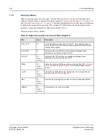
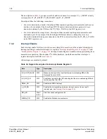
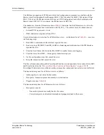
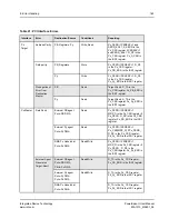
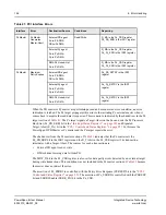
Interrupt Status Register 1 provides status for interrupts resulting from exceptions occurring during 
device operation. This includes maximum retry errors, bus errors, and parity error. A register 
description for ISR1 is provided in 

Table 35

.

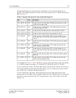
Table 35: Register Description for Interrupt Status Register 1

Bits

Type

Description

ISR0_ACTV

R

This bit allows software to monitor activity of the other interrupt status 
register while observing this interrupt status register. It essentially chains the 
two registers so both are only read if necessary.

PB_x_RETRY

R/

Write 1 
to Clear

The PowerSpan II PB Master Interface has detected more than the 
maximum allowable retries.

PB_x_ERR

R/

Write 1 
to Clear

The PowerSpan II PB Interface asserted (as slave) or received (as master) 
PB_TEA_. The PB slave detects illegal conditions, while the PB master 
receives PB_TEA_.

PB_A_PAR

R/

Write 1 
to Clear

An address parity error was detected on the PB.

PB_x_D_PAR

R/

Write 1 
to Clear

A data parity error was detected on the PB.

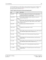
P2_x_ERR

R/

Write 1 
to Clear

The PowerSpan II PCI-2 Interface detected an error. The corresponding PCI 
Control and Status Register must be checked for the error.

P2_A_PAR

R/

Write 1 
to Clear

The PowerSpan II PCI-2 Interface detected an address parity error. 

P2_x_RETRY

R/

Write 1 
to Clear

The PowerSpan II PCI-2 Master has detected more than the maximum 
allowable retries.

P1_x_ERR

R/

Write 1 
to Clear

The PowerSpan II PCI-1 Interface detected an error. The corresponding PCI 
Control and Status Register must be checked for the error.

P1_A_PAR

R/

Write 1 
to Clear

The PowerSpan II PCI-1 Interface detected an address parity error. 

P1_x_RETRY

R/

Write 1 
to Clear

The PowerSpan II PCI-1 Master has detected more than the maximum 
allowable retries.

Summary of Contents for PowerSpan II

Page 1: ...ver Creek Valley Road San Jose California 95138 Telephone 800 345 7015 408 284 8200 FAX 408 284 2775 Printed in U S A 2009 Integrated Device Technology Inc PowerSpan II User Manual 80A1010_MA001_09 November 2009 ...

Page 2: ...MPLES CONTAINED IN ANY IDT PUBLICATION OR PUBLIC DISCLOSURE OR THAT IS CONTAINED ON ANY IDT INTERNET SITE IN NO EVENT WILL IDT BE LIABLE FOR ANY DIRECT CONSEQUENTIAL INCIDENTAL INDIRECT PUNITIVE OR SPECIAL DAMAGES HOWEVER THEY MAY ARISE AND EVEN IF IDT HAS BEEN PREVIOUSLY ADVISED ABOUT THE POSSIBILITY OF SUCH DAMAGES The code examples also may be subject to United States export control laws and ma...

Page 3: ... 5 2 I2C 27 1 6 Concurrent Reads 27 1 6 1 PowerSpan II s Concurrent Read Solution 27 1 6 2 PowerSpan II s Concurrent Read Applications 29 2 PCI Interface 31 2 1 1 Primary PCI 31 2 1 2 PCI Data Width 32 2 1 3 PCI Interface Descriptions 34 2 1 4 Transaction Ordering 34 2 2 PCI Target Interface 37 2 2 1 Address Phase 37 2 2 2 Data Phase 41 2 2 3 Termination Phase 44 2 3 PCI Master Interface 46 2 3 1 ...

Page 4: ...ss Phase 85 3 3 2 Data Phase 92 3 3 3 Terminations 98 3 4 PB Master Interface 100 3 4 1 Address Phase 100 3 4 2 Data Phase 103 3 4 3 Terminations 111 4 DMA 113 4 2 DMA Register Description 114 4 2 1 Source and Destination Addresses 114 4 2 2 Transfer Control Register 115 4 2 3 Command Packet Addressing 115 4 2 4 Address Retry 115 4 2 5 General DMA Control and Status 116 4 2 6 Processor Bus Transfe...

Page 5: ...rrupt Handling 145 7 2 Interrupt Sources 145 7 2 1 Interrupts from Normal Operations 145 7 2 2 Interrupts from Transaction Exceptions 146 7 3 Interrupt Registers 147 7 3 1 Interrupt Status 148 7 3 2 Interrupt Enable 150 7 3 3 Interrupt Mapping 152 7 4 Interrupt Pins 153 7 5 DMA Interrupts 154 7 5 1 DMA Interrupt Servicing 154 7 6 Mailboxes 154 7 7 Doorbells 155 8 Error Handling 157 8 2 PB Interfac...

Page 6: ...GA Pin Information 215 11 3 Single PCI PowerSpan II Pin Information 221 11 3 1 Single PCI PowerSpan II 420 HSBGA 221 11 3 2 420 HSBGA Pin Information 223 11 3 3 Single PCI PowerSpan II 484 HSBGA 227 12 Register Descriptions 235 12 1 Register Access 235 12 1 1 Register Map 235 12 1 2 Access from PCI 244 12 1 3 Access from the Processor Bus 245 12 1 4 Access from Multiple Interfaces 245 12 2 Registe...

Page 7: ...PowerSpan II Timing Parameters 396 15 3 Dual PCI PowerSpan II Timing Parameters 402 15 4 Timing Diagrams 408 16 Ordering Information 415 16 1 Ordering Information 415 A Hardware Implementation 417 A 2 Recommended Bootstrap Diode 417 A 3 PLL External Decoupling 418 A 3 1 Backwards Compatible PLL Decoupling for Migrating PowerSpan II Designs 418 A 3 2 PowerSpan II External PLL Decoupling for New Des...

Page 8: ...Contents 8 PowerSpan II User Manual 80A1010_MA001_09 Integrated Device Technology www idt com ...

Page 9: ...e 106 Figure 17 Direct Mode DMA Transfers 119 Figure 18 DMA Command Packet Linked List 122 Figure 19 Sequence of Operations in a Linked List Transfer 123 Figure 20 Assignment of Additional Bus Requesters with PCI Arbiters 138 Figure 21 Arbitration Algorithm 140 Figure 22 PowerSpan II Power up Waveform 174 Figure 23 PowerSpan II Configuration Slave Mode Timing 175 Figure 24 480 HSBGA 206 Figure 25 ...

Page 10: ...ser Manual 80A1010_MA001_09 Integrated Device Technology www idt com Figure 43 PowerSpan II in Multi processor 60x system 422 Figure 44 PowerSpan II in CompactPCI Peripheral Slot 424 Figure 45 PowerSpan II in CompactPCI System Slot 426 ...

Page 11: ...nt settings 96 Table 19 PowerSpan II PB Data Parity Assignments 97 Table 20 Default PowerSpan II PB Master Transfer Type 102 Table 21 PowerSpan II PB Address Parity Assignments 102 Table 22 PowerSpan II PB Transfer Sizes 104 Table 23 64 bit PB Data Bus Byte Lane Definitions 107 Table 24 PowerSpan II Processor Bus Single Beat Data Transfers 108 Table 25 PowerSpan II PB Data Parity Assignments 110 T...

Page 12: ...teristics 205 Table 61 Package Characteristics 213 Table 62 Package Characteristics 221 Table 63 Package Characteristics 227 Table 64 PowerSpan II Register Map 235 Table 65 Abbreviations used in Register Descriptions 248 Table 66 Read Amount Versus Read Command 256 Table 67 Block Size 271 Table 68 Setting for MODE and MEM_IO Bits 272 Table 69 Read Amount 273 Table 70 Arbitration Pin Mapping 274 Ta...

Page 13: ...ckage Performance 392 Table 95 Thermal Parameters 393 Table 96 480 PBGA Package Performance 393 Table 97 Reset and Clock Timing Parameters 396 Table 98 PCI 33 MHz Timing Parameters 398 Table 99 PCI 66 MHz Timing Parameters 399 Table 100 PB Timing Parameters 400 Table 101 Miscellaneous Timing Parameters 401 Table 102 Reset and Clock Timing Parameters 402 Table 103 PCI 33 MHz Timing Parameters 404 T...

Page 14: ...List of Tables 14 PowerSpan II User Manual 80A1010_MA001_09 Integrated Device Technology www idt com ...

Page 15: ...al Signal Notation Non differential signals are either active low or active high An active low signal has an active state of logic 0 or the lower voltage level and is denoted by a lowercase _ or for PCI signals An active high signal has an active state of logic 1 or the higher voltage level and is not denoted by a special character The following table illustrates the non differential signal naming...

Page 16: ...a product that is near production ready and is revised as required Formal Contains information about a final customer ready product and is available once the product is released to production Revision History 80A1010_MA001_09 Formal November 2009 This document was rebranded as IDT It does not include any technical changes 80A1010_MA001_08 Formal March 2007 The formatting of this document has been ...

Page 17: ...Manual 80A1010_MA001_09 Integrated Device Technology www idt com 80A1010_MA001_06 Formal December 2002 The Single PCI PowerSpan II has reached production status This manual represents the production information for the Single PCI PowerSpan II ...

Page 18: ...About this Document 18 PowerSpan II User Manual 80A1010_MA001_09 Integrated Device Technology www idt com ...

Page 19: ...new level of PCI bus switch flexibility The integrated non transparent PCI to PCI bridge in the Dual PCI PowerSpan II provides a significant opportunity for designers to reduce component count and increase overall system performance PowerSpan II offers a flexible package design The design is available in both the original PowerSpan package dimensions and newly designed smaller packages The high le...

Page 20: ...E1149 1 Boundary Scan Up to 7 External Bus Masters Up to 8 Slave Devices Hot Swap Friendly Programmable on PCI 1 or PCI 2 Up to 7 External Bus Masters Up to 3 External Bus Masters 32 bit Address 64 bit Data 100 MHz Processor Bus PowerPC Processor Bus Interface PB Arbiter PCI 1 Arbiter PCI 2 Arbiter PCI 1 Interface PCI 2 Interface Optional Interface JTAG Hot Swap Controller DMA Registers 32 bit Add...

Page 21: ...z 420 HSBGA 1 27mm ball pitch 35mm body size 484 PBGA 1 0mm ball pitch 23mm body size Dual PCI PowerSpan II CA91L8200B 32 bit 66MHz and 64 bit 66MHz 480 HSBGA 1 27mm ball pitch 37 5mm body size 504 HSBGA 1 0mm ball pitch 27mm body size 1 1 2 PowerSpan II Benefits PowerSpan II offers the following benefits to designers Smaller packages reduce board area required for system design Integrated PCI bus...

Page 22: ...elps designers working on infrastructure equipment in the following areas PowerSpan II is a very flexible device The following diagram shows a typical PowerPC system architecture using PowerQUICC II and the Dual PCI PowerSpan II Figure 2 Typical PowerSpan II Application Table 1 PowerSpan II Applications LAN WAN Remote Local Access Wireless Exchange Carrier Switching Equipment ADSL Concentrators Th...

Page 23: ... new ID Register Descriptions on page 235 Read implementation PowerSpan II supports 4 byte transactions PCI Interface on page 31 Processor Bus Interface on page 83 and Register Descriptions on page 235 True Little endian Mode A new endian mode was developed for PowerSpan II Endian Mapping on page 177 and Register Descriptions on page 235 Base Address Implementation PowerSpan II supports a PCI base...

Page 24: ...idging function is non transparent In a non transparent bridge one PCI bus is hidden from system BIOS running in the other PCI domain Memory and I O transfers pass freely between the PCI interfaces but Configuration accesses are filtered The application is shown in Figure 3 Programmable DMA Block Size PowerSpan II enables programmable DMA block sizes DMA on page 113 and Register Descriptions on pa...

Page 25: ...he PowerSpan II provides extra functionality for one of the PCI interfaces The PCI Interface assigned extra functionality must be specified as Primary PCI Interface through a power up option The Primary PCI Interface functions are CompactPCI Hot Swap Friendly support I2O 2 0 Specification compliant messaging Vital Product Data support This extra functionality is available for the Single PCI PowerS...

Page 26: ... methodology This verification ensures any potential interface issues are identified and resolved by IDT before PowerSpan II customers begin to design their own systems PowerSpan II supports processor 60x bus extended cycles on the Processor Interface Extended cycle support means more flexible bursting and more efficient use of the processor bandwidth 1 3 1 Address Decoding Instead of consuming ch...

Page 27: ...2 C bus compatible interface which supports up to eight I2 C slave devices This interface is used by PowerSpan II for the initialization of registers and for reading and writing PCI Vital Product Data VPD PowerSpan II also provides a mechanism to perform master read and write operations to EEPROMs or other I2C compatible slave devices 1 6 Concurrent Reads PowerSpan II s Switched PCI architecture e...

Page 28: ...y support two reads to the Processor Bus and two reads to the PCI bus 1 6 1 1 Conventional Reads and Retries In conventional FIFO based bridge architectures bus masters must take turns for read opportunities and incur multiple retries while waiting Figure illustrates the read process for subsequent reads where retries are incurred while a pending read is completed Master 1 Makes a read request and...

Page 29: ...receive only one retry before receiving read data Even with another read pending when the PCI Target Interface of the PCI host device receives a read request it latches the information and begins another burst read prefetch on the processor bus The PCI host bridge latches the addresses and delivers the data to each master using separate dedicated buffering This approach greatly reduces the overall...

Page 30: ...ending for the processor slave interface in the PCI bridge assuming there are two PowerQUICC IIs on the local bus This architecture adds considerable latencies to read transactions because of FCCs attempting reads to host memory across the PCI bus Ideally each FCC would have a dedicated channel to the PCI bus so they do not have to share resources PowerSpan II supports this ideal situation through...

Page 31: ... Silicon Support on page 53 Vital Product Data on page 60 I2O Shell Interface on page 62 2 1 Overview This chapter describes the functionality of the Dual PCI PowerSpan II The Single PCI PowerSpan II is identified when its functionality or settings differ from the Dual PCI PowerSpan II The Single PCI PowerSpan II and the Dual PCI PowerSpan II have different characteristics The features of each dev...

Page 32: ...e Primary PCI Interface The Primary PCI interface is enabled with a power up option see 9 Resets Clocks and Power up Options on page 167 2 1 1 1 Clock Frequencies Each of the PCI interfaces PCI 1 and PCI 2 run at frequencies from 25 MHz to 66 MHz The DEV66 bit in the PCI 1 Control and Status Register on page 251 indicates that PowerSpan II is a 66 MHz capable device The speed of these buses is det...

Page 33: ...see Table 3 2 1 2 3 PowerSpan II in Hot Swap Applications In Hot Swap applications the P1_64EN signal is the only signal sampled to indicate the PCI data width The following scenarios can be used for determining the proper implementation of the P1_REQ64 and P1_64EN signals PCI bus is currently a 32 bit slot and the Hot Swap board is 64 bit capable In this case P1_REQ64 is pulled up in the slot and...

Page 34: ... oscillate and that there is not a significant power drain through the input buffer 2 1 3 PCI Interface Descriptions The PowerSpan II PCI interfaces are described in terms of its PCI master and PCI target functions This description is largely independent of PCI 1 versus PCI 2 or the assignment of the Primary PCI Interface functions Exceptions to these rules are noted as required 2 1 4 Transaction ...

Page 35: ...e is a possibility that a transaction from PCI 2 can be queued ahead of a transaction from PCI This is caused by the fact there is no transaction ordering between the two independent PCI interfaces For example if transactions to the PB Interface arrive in the following order from PCI 1 and PCI 2 PCI 1 Write 1 PCI 2 Write 1 PCI 2 Write 2 PCI 1 Write 2 The transactions can be completed to the PB Int...

Page 36: ...riod This helps prevent PowerSpan II from interfering with processor bus instruction fetches All transactions writes reads DMA from two source interfaces arbitrate in a round robin scheme on a per interface basis Refer to Transactions Between the PB Interface and the PCI Interfaces on page 35 for more information 2 1 4 4 PCI Transaction Ordering Rules The PCI 2 2 Specification outlines transaction...

Page 37: ...e management Terminations This section describes the terminations supported by the PowerSpan II how they are mapped from the destination port to the PCI Target and exception handling 2 2 1 Address Phase The address phase deals with the decoding of PCI accesses 2 2 1 1 Transaction Decoding Transaction decoding on the PCI Target operates in both normal decode mode and Master based decode mode Only m...

Page 38: ...errupt Acknowledge No 0001 Special Cycle No 0010 I O Read No 0011 I O Write No 0100 Reserved N A 0101 Reserved N A 0110 Memory Read Yes 0111 Memory Write Yes 1000 Reserved N A 1001 Reserved N A 1010 Configuration Read Yes Type 0 only 1011 Configuration Write Yes Type 0 only 1100 Memory Read Multiple Yes 1101 Dual Address Cycle No 1110 Memory Read Line Yes 1111 Memory Write and Invalidate Aliased t...

Page 39: ...the corresponding image generates Memory Read commands on the destination PCI bus Py with the same byte enables latched from the source bus transaction PowerSpan II is capable of performing 1 2 3 or 4 byte memory transfers on the PCI bus es Default value is 0 Regular I O mode RTT 4 0 R W A 5 bit value defined in the processor bus protocol is generated on the PB_TT lines during a read on the proces...

Page 40: ...get image BS 3 0 in the PCI 1 Target Image x Control Register on page 268 translation address TADDR in the PCI 1 Target Image x Translation Address Register on page 274 When address translation is disabled the address on the destination bus is the same as the address on the source bus 2 2 1 3 Transaction Type Mapping A transaction can be mapped to the PB interface or to another PCI Interface MRA R...

Page 41: ...rs are reported on Px_SERR when both the Parity Error Response PERESP and SERR Enable SERR_EN bits are set in the PCI 1 Control and Status Register on page 251 Assertion of the Px_SERR signal can be disabled by clearing the SERR_EN bit PowerSpan II records an error condition in the event of an address parity error see Error Handling on page 157 PowerSpan II claims the errored transaction and forwa...

Page 42: ...tries requested data 3 Delayed Read Completion The master repeats the transaction with the same parameters used for the initial request and data is provided by PowerSpan II Read line buffers are allocated on a first come first serve basis When an external master makes the initial memory request the PowerSpan II PCI Target captures the PCI address in an available delayed read request latch This ini...

Page 43: ...ield up to 128 bytes The Memory Read Line command results in a prefetch of the value programmed into Cache Line CLINE bit When the MRA bit is cleared the target image prefetches 8 bytes when a PCI Memory Read command is decoded The Memory Read Multiple command results in a prefetch read of a minimum of 32 bytes or the value programmed into the RD_AMT 2 0 field independent of the MRA bit setting Th...

Page 44: ...rrors as a PCI target Data parity errors are reported through the assertion of Px_PERR when the PERESP bit is set The Detected Parity Error D_PE bit in the PCI 1 Control and Status Register on page 251 is set when PowerSpan II encounters a parity error as a PCI target on any transaction PowerSpan II records an error condition when a parity error occurs see Error Handling on page 157 2 2 3 Terminat...

Page 45: ...transaction by negating Px_DEVSEL and Px_TRDY and asserting Px_STOP on the same clock edge when it cannot respond to the transaction or during a fatal error A fatal error occurs when a bus error is experienced on the processor bus the maximum retry count is exceeded a Target Abort occurs on the alternate PCI bus during a read or a Master Abort occurs on the alternate PCI bus during a read Although...

Page 46: ...a PowerSpan II register access This section discusses only the first three conditions listed above Configuration and IACK cycles are discussed in Configuration and IACK Cycle Generation on page 246 The operation of the PCI Master is described by dividing the PCI master transaction into the following phases Arbitration phase This section describes how PowerSpan II requests the PCI bus and its respo...

Page 47: ...rface Arbitration on page 137 for more information The internal PowerSpan II PCI arbiter parks the bus on a PCI master by asserting Px_GNT to the PCI master Bus parking improves the performance of the PowerSpan II PCI Master by reducing arbitration latency 2 3 2 Address Phase The address phase deals with the generation of the PCI address and command encoding 2 3 2 1 Command Encoding The encoding o...

Page 48: ...ncoding for Transaction Type PowerSpan II as PCI Master Px_C BE 3 0 Transaction Type PowerSpan II Capable 0000 Interrupt Acknowledge Yes see Configuration and IACK Cycle Generation on page 246 0001 Special Cycle No 0010 I O Read Yes 0011 I O Write Yes 0100 Reserved N A 0101 Reserved N A 0110 Memory Read Yes 0111 Memory Write Yes 1000 Reserved N A 1001 Reserved N A 1010 Configuration Read Yes see C...

Page 49: ...bled by setting the TA_EN bit in PCI Target or PB Slave Image Control Register PowerSpan II produces the PCI address using the following inputs the incoming address from the source bus the block size of the slave or target image the translation offset For address translation going from the processor bus to PCI see Processor Bus Interface on page 83 For an example of address translation control goi...

Page 50: ...on page 304 When the Dual PCI PowerSpan II is used incoming PCI writes are executed as similar writes on the alternate PCI interface For example a 64 byte burst write to memory space from the PCI 1bus is executed as a 64 byte burst write to the memory space on the PCI 2 bus provided the target on PCI 2 does not disconnect DMA Writes The PowerSpan II DMA channels always attempt to perform the longe...

Page 51: ...ported through the assertion of Px_PERR when the PERESP bit is set The Detected Parity Error D_PE bit in the PCI 1 Control and Status Register on page 251 is set when PowerSpan II encounters a parity error as a PCI master on any transaction PowerSpan II records an error condition in the event of a parity error see Error Handling on page 157 The Master Data Parity Detected MDP_D bit in the PCI 1 Co...

Page 52: ... is high by the target because it cannot currently process the transaction Retry means the transaction is terminated after the address phase without data transfer PowerSpan II has a Maximum Retry Counter MAX_RETRY in the PCI 1 Miscellaneous Control and Status Register on page 283 which is used to record an error condition if the number of retries exceed the programmed amount see Error Handling on ...

Page 53: ...pport This support includes A 5V tolerant input pin HEALTHY for sensing the status of the Back End power on the card An input pin P1_64EN that enables Hot Swap adapter cards to sense the presence of a 64 bit PCI backplane 2 4 1 LED Support The LED can be controlled by hardware and software PowerSpan II drives the LED signal low to turn on the LED during the Physical and Hardware Connection process...

Page 54: ...ong medium short to allow power and ground signal and a Board Inserted Indicator BD_SEL to be connected and disconnected in stages A limited number of power and ground pins are long The rest of the power ground and signal pins are of medium length BD_SEL is a short pin When BD_SEL connects the physical connection process is complete 2 4 4 1 CompactPCI Hot Swap Process A CompactPCI Hot Swap board i...

Page 55: ...echarge Regulator 5 V 3 3v 2 5v P1_RST_DIR remaining PCI 1 I O PB_RST_DIR PB_CLK remaining PB I O P2_RST_DIR P2_CLK remaining PCI 2 I O GND LED ES Long Pins Ejector Switch Early Power 5 V 3 3 V HEALTHY GND Hot Swap Supply Sequencer 5 V 3 3 V Power On Reset Oscillator Regulator Back End Power 3 3 V 2 0 V CLKIN remaining I O GND Host Processor RST CLK remaining I O GND Secondary PCI 3 3 V BD_SEL HEA...

Page 56: ... in this case PCI 1 connects to the PCI pins on the backplane PowerSpan II P1_CLK is within specification 3 Short pins contact BD_SEL asserted Back End Power ramps Back End Power up reset asserted PowerSpan II PO_RST_ asserted Host processor PORESET_ asserted Host processor asserts HRESET_ Clock generator begins oscillation PowerSpan II PB_CLK and P2_CLK begin to oscillate Ejector switch closes so...

Page 57: ... Setting INS bit in the HS_CSR register Asserting ENUM 7 PowerSpan II is now able to accept Configuration cycles on PCI 1 from the CompactPCI Host Since Px_LOCKOUT bit in the PCI 1 Miscellaneous Control and Status Register on page 283 defaults to 1 PowerSpan II retries the Host Configuration accesses on the PCI 1 Interface until Px_LOCKOUT is cleared The Host then negates ENUM by clearing the Inse...

Page 58: ...in a software dormant state Sets the LED On Off LOO bit in the P1_HS_CSR register This causes the assertion of LED which turns the light emitting diode to signal the operator 3 Operator begins extracting the card At this point the operator can close the ejector switch and reenter the insertion process EXT bit INS bit LED ENUM Ejector State PCI Signals PCI Clock PCI RST HEALTHY BD_SEL Back End Powe...

Page 59: ... by the host the operator can close the ejector switch rather than extracting the card If the closure or the extraction occurs a PowerSpan II register reload from EEPROM does not occur EXT bit INS bit LED ENUM Ejector State PCI Signals PCI Clock PCI RST HEALTHY BD_SEL Back End Power Early Power Ejector Unlatched SW Clear EXT bit SW Set LOO bit Withdrawal Starts Short disengage Med disengage Long d...

Page 60: ...rs Of these bytes the first 64 bytes are VPD Read Only and the remaining 128 bytes are VPD Read Write When VPD_CS 0b000 VPD addresses are translated upward by 64 bytes before being presented to the EEPROM PowerSpan II can be programmed with an alternate chip select for VPD access if more than the 192 accessible bytes is required Programming of the I2C chip select is done in the PowerSpan II Miscel...

Page 61: ...ead operation the write operation always writes four consecutive bytes starting from the VPD address to the EEPROM The PCI 1 Vital Product Data Register on page 267 is written with the 4 bytes of data Byte 0 register bits 7 0 contains the data to be written to the location referenced by the VPD Address Bytes 1 3 contain the data for the successive bytes The VPDA field and the F bit is then written...

Page 62: ...ace consists of Inbound and Outbound Queues and supporting I2O Host interrupt registers The queues contain Message Frame Addresses MFAs These MFAs specify the starting address of Message Frames relative to the base address of the memory window in PowerPC memory PowerSpan II implements I2O support with the first Memory Base Address Register in PCI configuration space The I2O target image is divided...

Page 63: ... Queues 3 The PCI I2O target image must be configured to claim I2O Shell and Message Frame accesses from PCI The following registers must be programmed Configure I2O image size with the Block size BS bit in PCI I2O Target Image Control Register on page 352 PCI_TI2O_CTL Enable Base Address Register BAR visibility in configuration space Set BAR_EN in the PCI_TI2O_CTL register Program PCI Base Addres...

Page 64: ...four I2O defined memory mapped registers on PCI to enable the physical and logical connection of the IOP to the system Two of these memory mapped registers provide the interface for the external Host platform and other IOPs to exchange messages with the local IOP sitting behind the PowerSpan II These two registers are the Inbound Queue and Outbound Queue interfaces The other two registers are used...

Page 65: ...t List contains the MFAs of MFs in the Host system memory which contain outbound messages for the Host to process When the local IOP wishes to send a message to the Host platform it must first obtain an MFA from the Outbound Free List The local IOP is then free to place a message in the associated MF The MFA is then placed into the Outbound Post List for the Host to process All Outbound messages a...

Page 66: ...FIFO implemented in local memory Inbound Post List Bottom Bottom Increment Top Pointer Registers IPL_BOT IPL_BOT_INC IPL_TOP Used to manage the Inbound Post List circular FIFO implemented in local memory Outbound Free List Bottom Bottom Increment Top Pointer Registers OFL_BOT IPL_BOT_INC OFL_TOP Used to manage the Outbound Free List circular FIFO implemented in local memory Outbound Post List Bott...

Page 67: ...nter then equals the Bottom pointer a FIFO full condition exists After a FIFO read the Bottom pointer is incremented If the Bottom pointer then equals the Top pointer a FIFO empty condition exists PCI Bus Inbound Queue 0x040 Inbound Free List FIFO Inbound post List FIFO Outbound Free List FIFO Outbound Post List FIFO Bottom Pointer Top Pointer Bottom Pointer Top Pointer Top Pointer Bottom Pointer ...

Page 68: ...rite transaction on PCI and generate a write to the Inbound Post List FIFO at the local IOP memory address pointed to by the Inbound Post List Top Pointer Register PowerSpan II then increments the Inbound Post List Top Pointer Register and asserts the I2O_IOP Interrupt Status bit in the ISR0 register to notify the local processor of MFAs in the Inbound Post list FIFO The IPL bit in the I2O Control...

Page 69: ...he Outbound Post list FIFO PowerSpan II determines the Outbound Post List FIFO to be non empty when the Outbound Post List FIFO Bottom and Top pointers do not point to the same FIFO address 2 6 5 1 Host Processor Functions For Outbound Messaging the host processor performs the following detects the interrupt reads the I2O Outbound Post List Interrupt Status Register 0x030 reads the Outbound Queue ...

Page 70: ...es therefore the least significant four bits of the MFA are always zero The Pull options use these four bits to create an Extended MFA XMFA The Pull model uses the least significant bit of the XMFA to indicate a pull request This bit is the Pull Indicator or the P bit Bits 3 1 of the XMFA indicate the number of data transfers required to copy the message This number is system specific and has no e...

Page 71: ...When the IOP returns XMFAs to the Host Free List FIFO sets the P bit to 1 When the IOP reaches the end of the FIFO resets the FIFO index to the base address and this time through write the P bit to 0 This allows the Host to track the progress of the local IOP in returning XMFAs Figure 11 illustrates the following steps in PowerSpan II I20 pull capability 1 Host reads XMFA from Host Free List 2 Hos...

Page 72: ...ty PCI Bus Inbound Queue 0x040 Inbound Free List FIFO Inbound Post List FIFO Host Free List FIFO Bottom Pointer Top Pointer Bottom Pointer Top Pointer Top Pointer Bottom Pointer Local Processor IOP Inbound Queue Host Platform Host Free List Index Host Processor MFA Headroom XMFA XMFA Step 1 XMFA Step 3 Step 6 Step 4 Step 6 XMFA Step 5 Step 3 ...

Page 73: ...PowerSpan II IOP Outbound Index Register is initialized by the IOP with a value received along with the Host Outbound Post List FIFO Size through an IOP Message Outbound Extensions message from the Host The size of the Host Outbound Post List FIFO is specified in the HOPL_SIZE bit in the I2O_CSR register The PowerSpan II IOP Outbound Index Register points to the Top of the Host Outbound Post List ...

Page 74: ... to assert the Interrupt to the Host The Host will post empty MFAs back to the IOP by writing to the PowerSpan II s Outbound Queue Register 0x044 with the C bit set to zero PowerSpan II services the written MFA the same as a normal Outbound MFA being returned to the IOP Figure 12 illustrates the following steps in PowerSpan II I20 outbound capability 1 Local processor reads the Outbound Free List ...

Page 75: ...owerSpan II I2O Outbound Capability PCI Bus Host Outbound Post List FIFO Outbound Free List FIFO IOP Outbound Index Host Outbound Index Top Pointer Bottom Pointer Host Processor Host Platform Outbound Queue Outbound Queue 0x044 Local Processor IOP XMFA Step 1 XMFA Step 3 Step 5 Step 4 Step 5 XMFA Step 3 XMFA XMFA ...

Page 76: ...rmined by the size of the PowerSpan II I2O target image as defined by the PCI_I2O_CTL BS register The offset of the I2O Host Outbound Index Register is programmed in the I2O Host Outbound Index Offset Register HOST_OIO of the PowerSpan II Register Map The following tables show the I2O register definitions Table 10 PowerSpan II I20 Target Image Map Offset HEX Register Mnemonic Register Name 0x000 0...

Page 77: ...I to offset 0x30 from Px_BSI2O is destined for OPL_IS When the I20 messaging unit in PowerSpan II is not enabled the OPL_IS register is not visible to read or write access The register essentially disappears from all PowerSpan II memory maps Register Name OPL_IS Register Offset 030 PCI Bits Function PPC Bits 31 24 I2O Reserved 0 7 23 16 I2O Reserved 8 15 15 08 I2O Reserved 16 23 07 00 I2O Reserved...

Page 78: ...2O_EN 1 a memory access from PCI to offset 034h from Px_BSI2O is destined for OPL_IM When the I20 messaging unit in PowerSpan II is not enabled the OPL_IM register is not visible to read or write access The register essentially disappears from all PowerSpan II memory maps Register Name OPL_IM Register Offset 034 PCI Bits Function PPC Bits 31 24 I2O Reserved 0 7 23 16 I2O Reserved 8 15 15 08 I2O Re...

Page 79: ...he I20 Interface in PowerSpan II is not enabled the IN_Q register is not visible to read or write access The register essentially disappears from all PowerSpan II memory maps Register Name IN_Q Register Offset 040 PCI Bits Function PPC Bits 31 24 MFA 0 7 23 16 MFA 8 15 15 08 MFA 16 23 07 00 MFA 24 31 Name Type Reset By Reset State Function MFA 31 0 R W Px_RST 0 Inbound Message Frame Address The In...

Page 80: ...the cycle on the destination bus When the I20 Interface in PowerSpan II is not enabled the OUT_Q register is not visible to read or write access The register essentially disappears from all PowerSpan II memory maps Register Name OUT_Q Register Offset 044 PCI Bits Function PPC Bits 31 24 MFA 0 7 23 16 MFA 8 15 15 08 MFA 16 23 07 00 MFA 24 31 Name Type Reset By Reset State Function MFA 31 0 R W Px_R...

Page 81: ...address the Interrupt is cleared This feature is only supported if the I2O Outbound Option is enabled with the XI2O_EN bit in the I2O_CSR register and I2O_EN The HOPL_SIZE bit in the I2O_CSR register determines the alignment of this Index register The Register Offset is specified in the I2O Host Outbound Index Offset Register at offset 0x548 of the PowerSpan II Register Map The I2O Host Outbound I...

Page 82: ...2 PCI Interface 82 PowerSpan II User Manual 80A1010_MA001_09 Integrated Device Technology www idt com ...

Page 83: ...se interfaces are not identical for the most part the processor interface on the PowerSpan II is referred to simply as the Processor Bus PB The interface sections in this chapter highlight where the PowerSpan II operates differently to address specific processor requirements as the need arises An example of this different operation is the extended cycles with the PowerQUICC II 3 2 1 Terminology Th...

Page 84: ... described below by dividing the PB Slave transaction into the following different phases Address phase This section discusses the decoding of processor bus accesses Data transfer This section describes control of transaction length Terminations This section describes the terminations supported by PowerSpan II and exception handling Pull up resistors are not required on the processor bus address P...

Page 85: ... slave images can support the local bus traffic of four PowerQUICC II SCCs two threads of CPU traffic destined for PCI 1 and two threads destined for PCI 2 The specialty images are used for the generation of PCI Configuration cycles on PCI 1 and PCI 2 IACK reads on PCI 1 IACK reads on PCI 2 and PowerSpan II register accesses The PB slave image also controls how an incoming PB transaction is mapped...

Page 86: ...g PB transaction to either of PCI 1 or PCI 2 Defaults to PCI 1 MEM_IO R W Enables 1 2 3 or 4 byte memory reads on the PCI bus es Regular I O mode PRKEEP R W Enables PowerSpan II to keep prefetch read data over subsequent transactions Disabled END 1 0 R W Sets endian mapping to little endian PowerPC little endian or big endian Big endian is the default mode RD_AMT 2 0 R W Controls the prefetch read...

Page 87: ...n 3 3 1 2 Transfer Types The PB Slave only claims processor bus transactions with specific transfer types The supported transfer types consist of address only read and write They are defined in Table 13 All reads are treated as delayed reads and can be single cycle extended or bursts All writes are treated as posted writes and can be single cycle extended or bursts PowerSpan II handles address onl...

Page 88: ...ects the master from slow access times for information it requires However when a write is performed to a prefetched address a subsequent read could yield stale data In order to guarantee there is no stale data set the PRKEEP bit to 0 This function disables the internal buffer to ensure there is no stale data By setting this PRKEEP bit to 0 PowerSpan II is unable to perform PCI read prefetches and...

Page 89: ...after the assertion of PB_AACK_ and until it is able to assert PB_TA When ARTRY_EN has a value of 1 the PB Slave can assert PB_ARTRY_ The default setting is 0 ARTRY_EN is disabled The PB Interface has higher performance if the ARTRY_EN bit is enabled PowerSpan II s PB Master or another external master can gain access to the bus when PowerSpan II cannot assert PB_TA When ARTRY_EN is enabled the PB ...

Page 90: ...fset processor bus address and block size of the image Table 14 Translation Address Mapping PB_SIx_TADDR Processor Bus Address PB_A BS bit PB_SIx_CTL register Block Size 31 0 10011 2G 31 30 0 1 10010 1G 31 29 0 2 10001 512M 31 28 0 3 10000 256M 31 27 0 4 01111 128M 31 26 0 5 01110 64M 31 25 0 6 01101 32M 31 24 0 7 01100 16M 31 23 0 8 01011 8M 31 22 0 9 01010 4M 31 21 0 10 01001 2M 31 20 0 11 01000...

Page 91: ... In a joint application all memory accesses from the PowerQUICC II to PowerSpan II must be routed through the internal memory controller on the PowerQUICC II When the data is passed through the memory controller both address parity and data parity can be used in the system If accesses do not pass through the memory controller of the PowerQUICC II before reaching PowerSpan II and PowerSpan II has e...

Page 92: ...nment Embedded processor bus transfer sizes and alignments defined in Table 16 and Table 17 are supported by the PB Slave for transaction accesses The shaded table cells in Table 17 show transactions that support the PowerPC 7400 processor Table 17 lists the size and alignment transactions less than or equal to 8 bytes PowerSpan II register accesses are limited to 4 bytes or less Table 16 PowerSpa...

Page 93: ...IZ 0 3 A 29 31 Data Bus Byte Lanes 0 1 2 3 4 5 6 7 Byte 0001 000 D0 0001 001 D1 0001 010 D2 0001 011 D3 0001 100 D4 0001 101 D5 0001 110 D6 0001 111 D7 Half word 0010 000 D0 D1 0010 001 D1 D2 0010 010 D2 D3 0010 011 D3 D4 0010 100 D4 D5 0010 101 D5 D6 0010 110 D6 D7 Tri byte 0011 000 D0 D1 D2 0011 001 D1 D2 D3 0011 010 D2 D3 D4 0011 011 D3 D4 D5 0011 100 D4 D5 D6 0011 101 D5 D6 D7 ...

Page 94: ...ned boundary Any transfer greater than a single word must start or end on a word boundary Word 0100 000 D0 D1 D2 D3 0100 001 D1 D2 D3 D4 0100 010 D2 D3 D4 D5 0100 011 D3 D4 D5 D6 0100 100 D4 D5 D6 D7 Five bytes 0101 000 D0 D1 D2 D3 D4 0101 001 D1 D2 D3 D4 D5 0101 010 D2 D3 D4 D5 D6 0101 011 D3 D4 D5 D6 D7 Six bytes 0110 000 D0 D1 D2 D3 D4 D5 0110 001 D1 D2 D3 D4 D5 D6 0110 010 D2 D3 D4 D5 D6 D7 Se...

Page 95: ...egister on page 287 Delayed Reads The outstanding read is referred to as a delayed read Delayed reads consist of the following phases 1 Delayed Read Request PowerSpan II PB Slave latches transaction parameters and issues a retry 2 Delayed Read Completion The PB Slave obtains the requested data and completion status on the destination bus 3 Read Completion The master repeats the transaction with th...

Page 96: ...or bus The PB Interface can generate a 32 byte burst read with a starting address at the second third or fourth 8 byte quantity A cache wrap read always causes the PB slave to make a 32 byte read request from the destination PCI bus In other words PRKEEP and RD_AMT 2 0 have no effect There are instances where a read requires more data than that specified by RD_AMT Since PB slaves cannot terminate ...

Page 97: ...d Amount RD_AMT field in the Processor Bus Slave Image x Control Register on page 287 is read The Delayed Read Request latch is de allocated when the external processor bus master completes the transaction PRKEEP has no affect when PKEEP is set to 1 and ARTRY_EN is disabled A maximum of 32 bytes can be programmed in the RD_AMT field 3 3 2 5 Writes All writes are posted and are buffered separately ...

Page 98: ...owerSpan II and PowerSpan II has either or both address and data parity enabled then PowerSpan II reports parity errors on the transaction To enable or disable address parity in PowerSpan II set the Address Parity Enable AP_EN bit in the Processor Bus Slave Image x Control Register on page 287 To enable or disable data parity in PowerSpan II set the Data Parity Enable DP_EN bit in the Processor Bu...

Page 99: ... for PCI I O space access to registers designed to generate PCI Configuration or IACK commands see Configuration and IACK Cycle Generation on page 246 PowerSpan II also asserts PB_TEA_ if a read from PCI generates a Master Abort or Target Abort The assertion PB_TEA_ is enabled or disabled with the TEA Enable TEA_EN bit in the Processor Bus Miscellaneous Control and Status Register on page 304 3 3 ...

Page 100: ...ndicate address bus ownership after it receives a qualified bus grant for its address bus request A qualified bus grant assumes the following address bus grant asserted PB_ARTRY_ negated address bus not busy The PB Master negates PB_ABB_ for at least one clock after Address Acknowledge PB_AACK_ has been asserted by the slave This is true even if the arbiter parked the bus on PowerSpan II For examp...

Page 101: ...the masters must ensure the following actions are taken release bus request if it is asserted for at least one clock do not acquire the bus if presently granted do not assert bus request during the window of opportunity To ensure a transaction is retried systems assert PB_ARTRY_ at or before the first assertion of PB_TA_ This timing avoids a data tenure being terminated after data is transferred b...

Page 102: ...PB master transaction PB_TT is specified with the PCI target image or DMA channel registers The following registers control the parameter for write transactions WTT 4 0 field in the PCI 1 Target Image x Control Register on page 268 WTT 4 0 field in the DMA x Attributes Register on page 317 The following registers control the parameter for read transactions RTT 4 0 field in the PCI 1 Target Image x...

Page 103: ... PB_AP 3 If the DBG signal is asserted past the data tenure of a transaction the PB Master sees the assertion of the DBG signal as a new data tenure and re asserts PB_DBB_ External slaves must not indicate a successful data transfer with the assertion of PB_TA_ and or PB_DVAL_ earlier than two clocks after the assertion of PB_TS_ To ensure PowerQUICC II compliance with this rule the PowerQUICC II ...

Page 104: ...ions in Table 22 indicate transaction sizes that are unique to the PowerQUICC II The extended cycles supported by the PowerQUICC II are identified with an additional size pin Processor Bus Transfer Size PB_TSIZ 0 Extended cycles are enabled using the EXTCYC bit in the Processor Bus Miscellaneous Control and Status Register on page 304 The following figures Figure 13 and Figure 14 illustrate burst ...

Page 105: ... illustrate single cycle read and single cycle write transfers on the PB Master Interface PB_CLK PB_A 0 31 PB_AP 0 3 PB_TSIZ 0 3 PB_TT 0 4 PB_D 0 63 PB_DP 0 7 PB_TEA_ PB_TA_ PB_DVAL_ PB_DBB PB_DBG_IN_ PB_ARTRY_ PB_AACK_ PB_TBST_ PB_TS_ PB_ABB_ PB_BG 1 _ PB_BR 1 _ 0A PB_CLK PB_A 0 31 PB_AP 0 3 PB_TSIZ 0 3 PB_TT 0 4 PB_D 0 63 PB_DP 0 7 PB_TEA_ PB_TA_ PB_DVAL_ PB_DBB PB_DBG_IN_ PB_ARTRY_ PB_AACK PB_T...

Page 106: ...options The size and alignment combinations defined in Table 24 are supported by the PowerQUICC II PowerPC 7xx and PowerPC 750 processors This set includes transactions less than or equal to 8 bytes single beat transactions specific misaligned transactions extended transactions of 16 or 24 bytes burst of 32 bytes PB_CLK PB_A 0 31 PB_AP 0 3 PB_TSIZ 0 3 PB_TT 0 4 PB_D 0 63 PB_DP 0 7 PB_TEA_ PB_TA_ P...

Page 107: ...Byte Address PB Byte Lanes PB_A 29 31 Lane Number PowerSpan II Pins PowerQUICC II Pins PowerPC 7xx Pins WinPath Pins 000 0 PB_D 0 7 D 0 7 DH 0 7 H_DATA 63 56 001 1 PB_D 8 15 D 8 15 DH 8 15 H_DATA 55 48 010 2 PB_D 16 23 D 16 23 DH 16 23 H_DATA 47 40 011 3 PB_D 24 31 D 24 31 DH 24 31 H_DATA 39 32 100 4 PB_D 32 39 D 32 39 DL 0 7 H_DATA 31 24 101 5 PB_D 40 47 D 40 47 DL 8 15 H_DATA 23 16 110 6 PB_D 48...

Page 108: ...0 processor Table 24 PowerSpan II Processor Bus Single Beat Data Transfers Size TSIZ 0 3 A 29 31 Data Bus Byte Lanes 0 1 2 3 4 5 6 7 Byte 0001 000 D0 0001 001 D1 0001 010 D2 0001 011 D3 0001 100 D4 0001 101 D5 0001 110 D6 0001 111 D7 Half word 0010 000 D0 D1 0010 001 D1 D2 0010 010 D2 D3 0010 011 D3 D4 0010 100 D4 D5 0010 101 D5 D6 0010 110 D6 D7 Tri byte 0011 000 D0 D1 D2 0011 001 D1 D2 D3 0011 0...

Page 109: ...ned boundary Any transfer greater than a single word must start or end on a word boundary Word 0100 000 D0 D1 D2 D3 0100 001 D1 D2 D3 D4 0100 010 D2 D3 D4 D5 0100 011 D3 D4 D5 D6 0100 100 D4 D5 D6 D7 Five bytes 0101 000 D0 D1 D2 D3 D4 0101 001 D1 D2 D3 D4 D5 0101 010 D2 D3 D4 D5 D6 0101 011 D3 D4 D5 D6 D7 Six bytes 0110 000 D0 D1 D2 D3 D4 D5 0110 001 D1 D2 D3 D4 D5 D6 0110 010 D2 D3 D4 D5 D6 D7 Se...

Page 110: ...Processor Bus Control and Status register Parity generation and checking is provided for each byte of the data bus and for each data beat of the data tenure Data parity bit assignments are as defined in Table 25 The data parity bits PB_DP 0 7 are driven to the correct values for even or odd parity by the PB Master during writes If checking is enabled by setting the DP_EN bit the data parity bits P...

Page 111: ...rt the termination of extended cycles The external slave asserts this pin once for each successful 8 byte transfer PB_TA_ is asserted with PB_DVAL_ on the final transfer of the transaction The slave uses PB_TA_ and or PB_DVAL_ to insert wait states The PB master ignores PB_DVAL_ when the EXTCYC bit cleared in the Processor Bus Miscellaneous Control and Status Register on page 304 Transfer Error Ac...

Page 112: ...3 Processor Bus Interface 112 PowerSpan II User Manual 80A1010_MA001_09 Integrated Device Technology www idt com ...

Page 113: ...ta transfer between the three ports of the Dual PCI PowerSpan II Processor Bus Interface PB PCI Interface 1 PCI 1 and PCI Interface 2 PCI 2 The programming and operation of the four DMAs are the same This chapter discusses DMA operation within the context of a single channel In addition since the DMAs are able to transfer data from any port to any port the DMA discussion refers to source bus and d...

Page 114: ...es even the same bus as that used for the Source Address This register can be programmed in Direct mode or automatically loaded in Linked List mode Writing to this register while the DMA is in operation has no effect While the DMA is active this register provides the status of the current destination address This address is byte aligned The lower bits on the destination address are the same as the...

Page 115: ... 2 4 Address Retry The Address Retry Enable ARTRY_EN bit in the Processor Bus Miscellaneous Control and Status Register on page 304 controls PowerSpan II s assertion of PB_ARTRY_ during the servicing of transactions When the ARTRY_EN bit is set to 0 the PB Slave is disabled from generating address retries 4 2 4 1 DMA Addresses and Retries If a PowerSpan II DMA transaction is retried enough times t...

Page 116: ...mpletion of the current command packet Clear DACT R Provides status of DMA activity active or inactive Clear DBS 1 0 R W Controls the byte size of DMA transactions when DBS_EN is set to 1 Clear DBS_EN R W Enables byte size control of transactions generated by the DMA Channel Transaction size is based on the setting of the DBS field Clear OFF R W DMA Channel Off Counter number of PB clocks Controls...

Page 117: ...aching the transaction DONE R Write 1 to clear A status bit indicating if the DMA has been completed its Direct mode or Linked List mode Clear P1_ERR_EN R W Enables an interrupt if an error occurs on PCI 1 Disabled P2_ERR_EN R W Enables an interrupt if an error occurs on PCI 2 Do not program this bit if using the Single PCI PowerSpan II Disabled PB_ERR_EN R W Enables an interrupt if an error occur...

Page 118: ...ng conditions are met The CHAIN bit is zero which indicates a Direct mode operation All status bits in the DMA General Control and Status Register are cleared including P1_ERR P2_ERR PB_ERR STOP HALT DONE The CHAIN bit and status bits can be properly configured on the same register write which sets the GO bit The DMA channel delivers data from the source port to the destination port until DMA is s...

Page 119: ...e Technology www idt com Figure 17 Direct Mode DMA Transfers Program Source and destination addresses Transfer size and addresses Set GO bit Await termination of DMA Normal Termination More transfers required No Yes Handle error No Yes Done Ensure status bits are clear ...

Page 120: ...the STOP_REQ bit in the DMA x General Control and Status Register on page 314 When this occurs the channel stops attempting to buffer data from the source bus When the remaining buffered source data is written to the destination bus the STOP status bit is set The channel can be restarted by clearing the STOP status bit along with any other status bits and then writing a 1 to the GO bit 4 4 Linked ...

Page 121: ...e DMA is in operation has no effect While the DMA is active this register provides the status on the current source address This address is byte aligned DMAx_DST_ADDR The Destination Address Register can be programmed for an address on any one of the three PowerSpan II buses including the same bus as that used for the Source Address This register can be programmed in Direct mode or automatically l...

Page 122: ...urce or destination port 2 Configure DMAx_ATTR parameters and DMAx_GCSR 3 Set up the NCP 31 5 field to point to the first command packet 4 Ensure the BC 23 0 field in the DMA Transfer Control Register is 0 5 Clear all status bits in the DMA General Control and Status Register 6 Set the GO bit The steps to configure a Linked List mode DMA transfer are illustrated in Figure 19 Reserved DMAx_SRC_ADDR...

Page 123: ...ed with a non zero byte count in the DMA Transfer Control Register a Direct mode DMA transfer is initiated by PowerSpan II to clear the remaining byte count value Once that Direct mode transfer is complete the DMA then processes the linked list pointed to in the DMA Command Packet Pointer Register This mechanism allows the restart of a linked list transfer that has been stopped with the STOP_REQ b...

Page 124: ... be restarted by writing 1 to HALT bit to clear the HALT state the CHAIN bit to re initiate the Linked List mode and the GO bit to re activate the DMA 4 5 DMA Interrupts The PowerSpan II DMA supports a number of interrupt sources for each channel Individual enable and status bits exist for each source The status and enable bits are contained in the DMA x General Control and Status Register on page...

Page 125: ... is reached 4 6 3 Source Port Errors When an error occurs on the source port transactions initiated by the source port are terminated Any source data buffered in the PowerSpan II is written to the destination port and the appropriate DMAx_GCSR error bit is set Due to the pipelined nature of DMA channel requests additional Source port transaction activity may occur until all outstanding channel req...

Page 126: ...ot updated with command packet data See Error Handling on page 157 and Interrupt Handling on page 145 for a full description of error logging support and associated interrupt mapping options Each PowerSpan II external port has error log registers that provides additional diagnostic information to assist in error recovery These error log registers indicate when multiple errors occur due to the pipe...

Page 127: ...age 135 5 1 Overview PowerSpan II has a master only I2 C bus compatible interface which supports up to eight I2 C slave devices This interface is primarily used by PowerSpan II for the initialization of registers and for reading and writing PCI Vital Product Data VPD However PowerSpan II also provides a mechanism for processor bus and PCI masters to access the I2 C devices PowerSpan II I2 C Interf...

Page 128: ...ST_ a power up reset the register loading process is defined by Table 31 The first byte read from the EEPROM defines the loading option and is reflected in the EEPROM Load Option ELOAD_OPT field in the Miscellaneous Control and Status Register on page 318 at the conclusion of the loading process The loading options for EEPROM are short loading and long loading The short load consists of 29 bytes a...

Page 129: ...H PCI 1 Target image 0 prefetch indicator 2 P1_BST1 PRFTCH PCI 1 Target image 1 prefetch indicator 1 P1_BST2 PRFTCH PCI 1 Target image 2 prefetch indicator 0 P1_BST3 PRFTCH PCI 1 Target image 3 prefetch indicator 0x07 7 0 P1_SID SID 15 8 PCI 1 Subsystem ID bits 15 8 0x08 7 0 P1_SID SID 7 0 PCI 1 Subsystem ID bits 7 0 0x09 7 0 P1_SID SVID 15 8 PCI 1 Subsystem vendor ID bits 15 8 0x0A 7 0 P1_SID SVI...

Page 130: ...D 7 4 P1_TI0_CTL BS PCI 1 Target image 0 block size 3 0 P1_TI1_CTL BS PCI 1 Target image 1 block size 0x0E 7 4 P1_TI2_CTL BS PCI 1 Target image 2 block size 3 0 P1_TI3_CTL BS PCI 1 Target image 3 block size 0x0F 7 MISC_CSR VPD_EN PCI Vital Product Data enable 6 4 MISC_CSR VPD_CS 2 0 PCI Vital Product Data chip select 3 0 PowerSpan II Reserved 0x10 7 MISC_CSR P1_LOCKOUT PCI 1 Lockout 6 MISC_CSR P2_...

Page 131: ...rSpan II Reserved 3 0 PCI_I2O_CTL BS PCI I2O Target image block size 0x13 7 5 PowerSpan II Reserved 4 P2_BSI2O PRFTCH PCI 2 I2O target image prefetch indicator 3 P2_BST0 PRFTCH PCI 2 Target image 0 prefetch indicator 2 P2_BST1 PRFTCH PCI 2 Target image 1 prefetch indicator 1 P2_BST2 PRFTCH PCI 2 Target image 2 prefetch indicator 0 P2_BST3 PRFTCH PCI 2 Target image 3 prefetch indicator 0x14 7 0 P2_...

Page 132: ...3 0 P2_TI2_CTL BS PCI 2 Target image 2 block size 3 0 P2_TI3_CTL BS PCI 2 Target image 3 block size 0x1B 0x1F PowerSpan II Reserved End of short load long load continues 0x20 7 0 P1_ID DID 15 8 PCI 1 Device ID bits 15 8 0x21 7 0 P1_ID DID 7 0 PCI 1 Device ID bits 7 0 0x22 7 0 P1_ID VID 15 8 PCI 1 Vendor ID bits 15 8 0x23 7 0 P1_ID VID 7 0 PCI 1 Vendor ID bits 7 0 0x24 7 0 P1_CLASS BASE PCI 1 Base ...

Page 133: ...s bits 15 12 3 PB_SI0_TADDR M3 PB Slave image 0 master 3 select 2 PB_SI0_TADDR M2 PB Slave image 0 master 2 select 1 PB_SI0_TADDR M1 PB Slave image 0 master 1 select 0 PowerSpan II Reserved 0x2E 7 0 PB_SI0_BADDR 31 24 PB Slave image 0 base address bits 31 24 0x2F 7 0 PB_SI0_BADDR 23 16 PB Slave image 0 base address bits 23 16 0x30 7 4 PB_SI0_BADDR 15 12 PB Slave image 0 base address bits 15 12 3 0...

Page 134: ...dated with EEPROM contents See Register Descriptions on page 235 for more information 0x35 7 0 P2_ID DID 7 0 PCI 2 Device ID bits 7 0 0x36 7 0 P2_ID VID 15 8 PCI 2 Vendor ID bits 15 8 0x37 7 0 P2_ID VID 7 0 PCI 2 Vendor ID bits 7 0 0x38 7 0 P2_CLASS BASE PCI 2 Base Class Code 0x39 7 0 P2_CLASS SUB PCI 2 Sub Class Code 0x3A 7 0 P2_CLASS PROG PCI 2 Programming Interface 0x3B 7 0 P2_CLASS RID PCI 2 R...

Page 135: ...performing a write or read access the user must poll the active bit until it is negated before performing other transfers The active bit is also asserted during power up EEPROM load and when a PCI Vital Product Data transfer is in progress Error ERR If the PowerSpan II is unable to complete an I2C access the ERR bit is set when the ACT is negated The ERR bit must be cleared before attempting anoth...

Page 136: ...first EEPROM then the address in the P1_VPDC or P2_VPDC register is used directly as the 8 bit EEPROM address Accesses to Vital Product Data in external EEPROM is performed in the manner described in Bus Master I2C Transactions on page 135 The bit ordering of the data returned from EEPROM in the PCI 1 Vital Product Data Register on page 267 can be addressed according to little endian or big endian...

Page 137: ...ach PCI interface PCI 1 and PCI 2 There is also one arbiter for the Processor Bus Interface 6 2 PCI Interface Arbitration Each PowerSpan II PCI Interface supports a PCI central arbiter Each arbiter has dedicated support for the PowerSpan II PCI Master with internal request and grant signaling and up to four external PCI masters PowerSpan II provides external pins to support three additional extern...

Page 138: ...n arbitration algorithm among the PCI masters assigned to each level For example all the PCI masters assigned to the lower priority level represent one entry in the higher priority round robin arbitration For every turn of the high priority round robin arbitration high priority PCI masters asserting Px_REQ are granted access to the PCI bus At the same time only one lower priority level PCI master ...

Page 139: ...e arbiter to be functioning and the PCI Master is included in the arbitration algorithm used by PowerSpan II When PowerSpan II is reset all masters are considered functioning the STATUS bit is set to 0 Refer to Bus Parking on a Non functioning Master on page 141 for more information on bus parking on a master that is non functioning 6 2 1 3 PCI Master Driving the PCI Bus A PCI master accessing the...

Page 140: ...see Resets Clocks and Power up Options on page 167 Each master has a arbitration level for PCI Master Device x Mx_PRI bit in the PCI 1 Bus Arbiter Control Register on page 284 Px_ARB_CTRL to determine its arbitration level External Arbitration When an external arbiter is used the PowerSpan II PCI Master uses Px_REQ 1 Px_GNT 1 to acquire the bus Master X Master Y Master Z Level 0 Master C Level 0 M...

Page 141: ...nctioning and Non functioning PCI Masters on page 139 for a detailed description of functioning and non functioning PCI Masters When PowerSpan II parks the bus on a non functioning PCI Master the PowerSpan II PCIx Arbiter waits for another master to request the bus Once another master request the bus the PCIx Arbiter then ignores the non functioning master until the master is considered functionin...

Page 142: ...ng the address bus the processor bus arbiter can park on either the Last bus master Specific bus master The bus parking mode is determined by the PARK bit in the PB_ARB_CTRL Register When specific master mode is selected PARK 0 the BM_PARK 1 0 field selects the specific bus master for address parking 6 3 2 Data Bus Arbitration The arbiter samples PB_TT 3 when PB_TS_ is asserted to generate data bu...

Page 143: ...s that the processor bus master the at receives the grant qualifies the grant The 7400_MODE bit is a power up option 6 3 3 Address Only Cycles The arbiter supports address only cycles If Transfer Type PB_TT 3 is sampled low during PB_TS_ the arbiter does not grant the data bus The use of PB_TT 3 as a data bus request means that the PowerSpan II PB arbiter does not support the processor bus instruc...

Page 144: ...processor bus boot The PWRUP_BOOT option sets the M1_EN bit in the PB_ARB_CTL register and the P1_LOCKOUT and P2_LOCKOUT bits in the MISC_CSR register Setting the Px_LOCKOUT bits means any configuration cycles for PowerSpan II on the PCI bus are retried until the Px_LOCKOUT bits are cleared from the processor bus or the EEPROM When PCI_BOOT is set to 1 boot is from PCI the Px_LOCKOUT bits are not ...

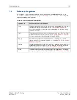
Page 145: ...4 Doorbells on page 155 7 1 Overview PowerSpan II handles interrupts both from normal device operation and from exceptions These interrupts are programmed through certain register settings and are signaled through both input and output signal pins The following sections describes PowerSpan II interrupt handling 7 2 Interrupt Sources Interrupt sources are classified as originating from normal devic...

Page 146: ...transaction through the interrupt enabling and status function Interrupt sources associated with exceptions are 1 PB Interface errors PB_P1_ERR PB_P2_ERR PB_A_PAR PB_P1_D_PAR PB_P2_D_PAR PB_P1_RETRY PB_P2_RETRY PB_PB_ERR PB_PB_D_PAR PB_PB_RETRY 2 PCI 1 Interface errors P1_PB_ERR P1_P2_ERR P1_A_PAR P1_PB_RETRY P1_P2_RETRY P1_P1_ERR P1_P1_RETRY 3 PCI 2 Interface errors P2_PB_ERR P2_P1_ERR P2_A_PAR P...

Page 147: ...eared by setting R Write 1 to Clear Enable The enable register bits cover all of the interrupt sources supported by PowerSpan II and allow status bits to assert an external pin see Interrupt Enable on page 150 With some exceptions all bits in these registers are Read Write Mapping This series of registers allow each interrupt source to be mapped to a specific interrupt output pin The mapping defin...

Page 148: ...Description ISR1_ACTV R This bit indicates an active status bit in ISR1 This enables software to monitor activity of the other interrupt status register while observing this interrupt status register I2O_HOST R Indicates to the Host that there are outstanding Message Frame Addresses in the Outbound Post List FIFO I2O_IOP R Write 1 to Clear Indicates to the IOP that there are outstanding Message Fr...

Page 149: ...B Interface asserted as slave or received as master PB_TEA_ The PB slave detects illegal conditions while the PB master receives PB_TEA_ PB_A_PAR R Write 1 to Clear An address parity error was detected on the PB PB_x_D_PAR R Write 1 to Clear A data parity error was detected on the PB P2_x_ERR R Write 1 to Clear The PowerSpan II PCI 2 Interface detected an error The corresponding PCI Control and St...

Page 150: ... 2 Interrupt Enable Each interrupt enable bit allows an active source status bit to assert one of the external interrupt pins Interrupt enabling is controlled through two registers Interrupt Enable Register 0 on page 332 and Interrupt Status Register 1 on page 329 Interrupt Enable Register 0 enables interrupts resulting from normal device operation This includes I2 O DMA hardware doorbell and mail...

Page 151: ...le 37 Register Description for Interrupt Enable Register 1 Bits Type Description PB_x_RETRY_EN R W Enables interrupt if the PowerSpan II PB Master has detected more than the maximum allowable retries PB_x_ERR_EN R W Enables interrupt if the PowerSpan II PB Interface asserted as slave or received as master PB_TEA_ PB_A_PAR_EN R W Enables interrupt if an address parity error was detected on the PB P...

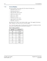
Page 152: ... IMR_PB Processor Bus sources IMR2_PB Processor Bus sources IMR_MISC I2O sources Each interrupt source contains a three bit field in an IMR_x register This mapping field determines which external pin to assert when the source is active and enabled Table 38 details the mapping scheme The shaded area in the table denotes the shaded map field and interrupt pin information apply only to the Dual PCI P...

Page 153: ... as inputs by default P1_INTA and P2_INTA are intended to be used with PCI interfaces PCI 1 and PCI 2 They are electrically PCI compliant To configure PCI interface Px with interrupt capability the following register settings are required INT_PIN 0x01 in the PCI 1 Miscellaneous 1 Register on page 262 Px_MISC1 This setting enables a single function PCI device INTA Px_HW_DIR 0x01 in the Interrupt Di...

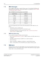
Page 154: ... 1 DMA Interrupt Servicing To service a DMA interrupt the following steps must be taken Read Interrupt Enable Register 0 on page 332 ISR0 to determine which DMA channel caused the interrupt Read DMAx_GCSR to determine which DMA source caused the interrupt Service the interrupt Write 1 to clear DMAx_GCSR status_bit and allow a restart of the DMA channel Write 1 to clear the DMAx_EN bit in the ISR0 ...

Page 155: ...t com 7 7 Doorbells The Doorbell interrupts are generated by writing 1 to the corresponding Doorbell x Enable DBx_EN bit in the Interrupt Enable Register 0 on page 332 The Doorbell interrupt is cleared by writing a 1 to the corresponding Doorbell x DBx bit in the Interrupt Status Register 0 on page 327 ...

Page 156: ...7 Interrupt Handling 156 PowerSpan II User Manual 80A1010_MA001_09 Integrated Device Technology www idt com ...

Page 157: ... 158 PCI Interface Errors on page 162 DMA Errors on page 166 8 1 Overview PowerSpan II has error detection error reporting and error recovery mechanisms for each of the major interfaces Processor Bus PB PCI 1 and PCI 2 The master and target slave of each interface provides error detection for transactions where they participate The types of errors identified are Address parity Data parity Bus erro...

Page 158: ...ror on a transaction destined for an agent connected to the PCI 1 external interface the PB_P1_D_PAR bit in the ISR1 is set Each PowerSpan II DMA channel provides an additional reporting mechanism see DMA Errors on page 166 8 2 PB Interface Errors The PB master and slave detect error conditions while participating in PB transactions In addition to Interrupt Status Register 1 the PB Interface has t...

Page 159: ...register Data parity PCI 1 Registers Write PB_P1_D_PAR in the ISR1 register PCI 2 Write PB_P2_D_PAR in the ISR1 register Illegal access PCI 1 Memory Unaligned access in PPC little endian mode PB_TEA if TEA_EN 1 PB_P1_ERR in the ISR1 register PCI 1 Configuration IO IACK Registers Unaligned access in PPC little endian mode Transaction Size 4 bytes or burst PCI 2 Memory Unaligned access in PPC little...

Page 160: ...rns to retrieve the read data it requested The assertion of the PB_TEA_ signal is controlled with assertion the Transfer Error Acknowledge Enable TEA_EN bit in the PB_MISC_CSR register If TEA_EN is set the PB slave reports error scenarios as defined in Table 40 If TEA_EN is cleared transactions determined to be in error are not forwarded to the intended interface or registers The appropriate ISR1 ...

Page 161: ...ce reported the error 2 Read error logs PB_ERRCS and PB_AERR to obtain diagnostic information if the PB Interface reported the error 3 Clear the Error Status ES bit in the PB_ERRCS to enable future error logging 4 Clear the status bit in ISR1 this negates external interrupt pin 5 Fix the configuration issue that caused the error 6 Retry the transaction that caused the error The flow of transaction...

Page 162: ...cipating in PCI bus transactions In addition to the Interrupt Status Register 1 on page 329 ISR1 the Px Interface provides the following reporting mechanisms External signaling of the following signals Target Abort Master Abort Address parity errors Data parity errors Detection of Target Abort Standard PCI error reporting in PCI 1 Control and Status Register on page 251 Px_CSR Capture of specific ...

Page 163: ...y Read Target Abort S_TA in the Px_CSR register Px_Py_ERR in the ISR1 register Px Master Data Parity External PB agent Px to PB DMA Read Px_PERR if PERESP 1 MDP_D in the Px_CSR register if Px_PERR D_PE in the Px_CSR register Px_PB_ERR in the ISR1 register External Py agent Px to Py DMA Read Px_PERR if PERESP 1 Px_CSR MDP_D if Px_PERR_ D_PE in the Px_CSR register Px_Py_ERR in the ISR1 register DMA ...

Page 164: ...PB agent read or write DMA channel moving data to from PB The MDP_D bit in the Px_CSR register is also set for data parity errors detected by an external target during write transactions This condition was not included in the Px master section of Table 41 because the master does not detect the error The assertion of Px_PERR is controlled with the Parity Error Response PERESP bit in the PCI 1 Contr...

Page 165: ...gging 4 Clear the status bit in ISR1 Negates external interrupt pin 5 Clear the error bits in Px_CSR 6 Fix the configuration issue that caused the error 7 Retry the transaction that caused the error The flow of transactions through PowerSpan II is independent of error status bits in Interrupt Status Register 1 on page 329 error status bits in PCI 1 Control and Status Register on page 251 and the E...

Page 166: ...rtion of a PowerSpan II interrupt pin according to Interrupt Handling on page 145 Assume that an error occurred at the PCI 1 master using DMA 2 A typical interrupt service routine executes the following steps 1 ISR1 read to determine which interface reported the error 2 If PCI 1 reports the error Error logs P1_ERRCS and P1_AERR read to obtain diagnostic information P1_CSR read to distinguish addre...

Page 167: ...l pins indicate a reset condition when driven low except for HEALTHY signal 9 1 1 1 Reset Direction Control Pins Each bidirectional reset pin PB_RST_ P1_RST and P2_RST has a dedicated direction control pin The assertion of a reset pin configured as input propagates to the other bus reset pins configured as output PowerSpan II has reset capabilities for PCI Host Adapter and Hot Swap applications Ta...

Page 168: ...sources are affected by active reset pins Table 43 Reset Direction Control Pins Control Pin Associated Reset Pin Description PB_RST_DIR PB_RST_ Direction of PB_RST_ When PB_RST_DIR 0 PB_RST_ is an input When PB_RST_DIR 1 PB_RST_ is an output P1_RST_DIR P1_RST Direction of P1_RST When P1_RST_DIR 0 P1_RST is an input When P1_RST_DIR 1 P1_RST is an output P2_RST_DIR P2_RST Direction of P2_RST When P2...

Page 169: ...ed see Table 97 on page 396 and Table 102 on page 402 parameter t103 The HEALTHY pin tristates all of PowerSpan II s output buffers and inhibits all of PowerSpan II s input buffers See CompactPCI Hot Swap Silicon Support on page 53 for more details on the use of HEALTHY The assertion of TRST_ resets the JTAG controller and configures the Boundary Scan Register for normal system operation 9 1 1 3 R...

Page 170: ...n page 396 and Table 102 on page 402 parameter t102 PowerSpan II PLLs are reset during either the assertion of PO_RST_ or the negation of HEALTHY The PLLs are not locked until a certain period after the negation of PO_RST_ or HEALTHY see Table 97 on page 396 and Table 102 on page 402 parameter t103 Each PLL has a dedicated configuration pin to indicate the desired operating frequency range The fol...

Page 171: ...n master functionality Power up option status can be confirmed by reading the Reset Control and Status RST_CSR register see Configuration Slave Mode on page 175 for more information Table 45 lists PowerSpan II power up options and directions for their configuration with PowerSpan II system pins and the processor data bus in configuration slave mode Power up options are not affected by reset events...

Page 172: ... requirements refer to Arbitration on page 137 for more information By enabling option PWRUP_BYPASS_EN all PLLs in the design are bypassed Typically this option must be disabled PLL in use in the system In the Single PCI PowerSpan II the following power up options are not configurable PWRUP_P2_ARB_EN no PCI 2 arbiter PCI 1 REQ64 Enable PWRUP_P1_R64_EN Disable P1_REQ64_ INT 4 _ 1 PB_D 4 0 P1_R64_EN...

Page 173: ...z and 50 MHz P1_M66EN Signal High when the PCI 1 clock frequency is 66 MHz Low when the PCI 1 clock frequency is 33 MHz P2_M66EN signal High when the PCI 2 clock frequency is 66 MHz Low when the PCI 2 clock frequency is 33 MHz There is a 10 ns minimum input setup time and 10 ns maximum input hold time requirement for latching these frequency range pins for determining the PLL range see Table 97 on...

Page 174: ...1 signals are used as general purpose interrupt pins Normal operation of these pins as interrupt pins requires external pull ups Default values for power up options loaded by INT 5 1 _ are shown in Table 45 Figure 22 PowerSpan II Power up Waveform Tip The logic levels are typically provided by external transceiver or FPGA when INT 5 1 are also used for general purpose I O pins PO_RST_ PB_HRESET_ P...

Page 175: ...guration master HRESET_ signal PB_D is connected to the processor bus data line The configuration slave power up options are configured by PB_D as defined in Table 45 PowerSpan II configuration slave mode timing is illustrated in Figure 23 Figure 23 PowerSpan II Configuration Slave Mode Timing The configuration master updates all configuration slaves for each HRESET_ sequence PowerSpan II updates ...

Page 176: ...9 Resets Clocks and Power up Options 176 PowerSpan II User Manual 80A1010_MA001_09 Integrated Device Technology www idt com ...

Page 177: ...essor Bus and PowerSpan II Register Transfers on page 179 Processor Bus and PCI Transfers on page 183 10 1 Overview PowerSpan II supports a flexible endian conversion scheme for the following transactions involving the Processor Bus PB Interface Access of PowerSpan II registers from the PB Interface Transfers between the processor bus and PCI both externally initiated and PowerSpan II DMA initiate...

Page 178: ...1_AD 15 8 0 1 Px_AD 15 8 010 2 P1_AD 23 16 0 2 Px_AD 23 16 011 3 P1_AD 31 24 0 3 Px_AD 31 24 100 4 P1_AD 39 32 1 0 Px_AD 7 0 101 5 P1_AD 47 40 1 1 Px_AD 15 8 110 6 P1_AD 55 48 1 2 Px_AD 23 16 111 7 P1_AD 63 56 1 3 Px_AD 31 24 Table 47 64 bit PB Data Bus Byte Lane Definitions Byte Address Processor Bus Byte Lanes PB_A 29 31 Lane Number PowerSpan II Pins PowerQUICC II Pins PowerPC 7xx Pins 000 0 PB_...

Page 179: ... page 295 The default mode is big endian which matches the default mode of the processor bus PowerSpan II registers are little endian structures The endian conversion process provided by PowerSpan II for processor bus accesses to its registers is designed to preserve the significance of the programmer s multi byte structures or scalars Endian conversion for access to PowerSpan II registers from th...

Page 180: ...ster Address A 2 A 1 0 0 1 2 3 4 5 6 7 11 10 01 00 Byte 000 D0 0 D0 001 D1 0 D1 010 D2 0 D2 011 D3 0 D3 100 D4 1 D4 101 D5 1 D5 110 D6 1 D6 111 D7 1 D7 Two bytes 000 D0 D1 0 D0 D1 001 D1 D2 0 D1 D2 010 D2 D3 0 D2 D3 100 D4 D5 1 D4 D5 101 D5 D6 1 D5 D6 110 D6 D7 1 D6 D7 Tri byte 000 D0 D1 D2 0 D0 D1 D2 001 D1 D2 D3 0 D1 D2 D3 100 D4 D5 D6 1 D4 D5 D6 101 D5 D6 D7 1 D5 D6 D7 Word 000 D0 D1 D2 D3 0 D0...

Page 181: ... processor is illustrated in Table 49 When the processor bus is operating in PowerPC little endian mode END bit must be set to PowerPC little endian mode In this case the PB Slave munges the processor bus address and maps byte lanes to register addresses to preserve the significance of the scalar Tip Munging the address makes the address appear to the processor bus that individual aligned scalars ...

Page 182: ... Processor Bus to PCI 2 Interrupt Acknowledge Cycle Generation register PB_P2_IACK The endian conversion scheme applied for processor bus access to these registers is controlled by the END bit but the endian mapping scheme in this case is described in Processor Bus and PCI Transfers on page 183 Table 50 PowerSpan II PowerPC Little Endian PB Register Accesses Transfer Size Starting Address Munged P...

Page 183: ... in the Processor Bus Slave Image x Control Register on page 287 END 1 0 field in the DMA x Transfer Control Register on page 311 The endian conversion mode of a DMA channel can be updated for each direct mode transaction or for each element in a linked list The following sections describe each of the endian conversion modes 10 4 1 Big endian Mode When operating in big endian mode PowerSpan II use...

Page 184: ...2 D2 011 D3 D3 100 D4 D4 101 D5 D5 110 D6 D6 111 D7 D7 Two bytes 000 D0 D1 D1 D0 001 D1 D2 D2 D1 010 D2 D3 D3 D2 100 D4 D5 D5 D4 101 D5 D6 D6 D5 110 D6 D7 D7 D6 Tri byte 000 D0 D1 D2 D2 D1 D0 001 D1 D2 D3 D3 D2 D1 100 D4 D5 D6 D6 D5 D4 101 D5 D6 D7 D7 D6 D5 Word 000 D0 D1 D2 D3 D3 D2 D1 D0 100 D4 D5 D6 D7 D7 D6 D5 D4 Five bytes 000 D0 D1 D2 D3 D4 D4 D3 D2 D1 D0 011 D3 D4 D5 D6 D7 D7 D6 D5 D4 D3 Si...

Page 185: ...actions When performing 4 byte transactions to the PCI bus in little endian mode the intended address must XOR the address with 0x4 This creates the address for PCI which is used in the transaction In little endian mode for 4 byte transfers the following changes must be made Change a register on PCI at offset 0x0 using address 0x4 Change a register on PCI at offset 0x4 using address 0x0 Change a r...

Page 186: ...D2 D2 011 D3 D3 100 D4 D4 101 D5 D5 110 D6 D6 111 D7 D7 Two bytes 000 D0 D1 D0 D1 001 D1 D2 D1 D2 010 D2 D3 D2 D3 100 D4 D5 D4 D5 101 D5 D6 D5 D6 110 D6 D7 D6 D7 Tri byte 000 D0 D1 D2 D0 D1 D2 001 D1 D2 D3 D1 D2 D3 100 D4 D5 D6 D4 D5 D6 101 D5 D6 D7 D5 D6 D7 Word 000 D0 D1 D2 D3 D0 D1 D2 D3 100 D4 D5 D6 D7 D4 D5 D6 D7 Five bytes 000 D0 D1 D2 D3 D4 D0 D1 D2 D3 D4 011 D3 D4 D5 D6 D7 D3 D4 D5 D6 D7 S...

Page 187: ...equests into single byte transactions on the processor bus with a performance penalty The PB Slave asserts PB_TEA_ in response to a transaction that is not naturally aligned These cases are as follows PB_TSIZ 3 5 6 7 bytes PB_TSIZ 2 bytes and PB_A 31 1 For DMA transactions between the processor 60x bus and the PCI 1 bus the END bit in the DMA x Transfer Control Register on page 311 must be set to ...

Page 188: ...tain addressing rules which must be followed In PowerSpan II when true little endian mode is selected no address swapping takes place refer to Table 53 This means that the MSB on the processor bus goes to the MSB on PCI However the MSB on processor bus is the low address and MSB on PCI is the high address True little endian mode cannot be used with the 4 byte read implementation in the PowerSpan I...

Page 189: ... 0 1 2 3 4 5 6 7 11 10 01 00 Byte 000 D0 0 D0 001 D1 0 D1 010 D2 0 D2 011 D3 0 D3 100 D4 1 D4 101 D5 1 D5 110 D6 1 D6 111 D7 1 D7 Two bytes 000 D0 D1 0 D0 D1 010 D2 D3 0 D2 D3 100 D4 D5 1 D4 D5 110 D6 D7 1 D6 D7 Tri bytes 000 D0 D1 D2 0 D0 D1 D2 001 D1 D2 D3 0 D1 D2 D3 100 D4 D5 D6 1 D4 D5 D6 101 D5 D6 D7 1 D5 D6 D7 Word 000 D0 D1 D2 D3 0 D0 D1 D2 D3 100 D4 D5 D6 D7 1 D4 D5 D6 D7 Five Bytes 000 D0...

Page 190: ...D2 D3 1 D4 D5 D6 D7 Seven Bytes 000 D0 D1 D2 D3 D4 D5 D6 0 D0 D1 D2 D3 1 D4 D5 D6 001 D1 D2 D3 D4 D5 D6 D7 0 D1 D2 D3 1 D4 D5 D6 D7 Double 000 D0 D1 D2 D3 D4 D5 D6 D7 0 D0 D1 D2 D3 1 D4 D5 D6 D7 Table 53 PowerSpan II True Little Endian Byte Lane Mappings Transfer Size Starting Address Munged PB_A 29 31 PowerPC Byte Lanes PowerSpan II PCI Address A 2 A 1 0 0 1 2 3 4 5 6 7 11 10 01 00 ...

Page 191: ...ese signal groupings The Single PCI PowerSpan II device does not implement the PCI 2 signal group 11 1 1 Signal Types Signals are classified according to the types defined in Table 54 Table 54 Signal Type Definitions Signal type Signal type definition Input Standard input only signal Output Standard output only signal Tristate output Standard tristate output only signal Open drain Open drain outpu...

Page 192: ...idirectional Hi Z Pull up resistor Address Parity The processor address bus master drives this signal to indicate the parity of the address bus PB_ARTRY_ Tristate bidirectional Hi Z Pull up resistor Address Retry Assertion of this signal indicates that the bus transaction must be retried by the processor bus master PB_A 0 31 Tristate bidirectional Hi Z No requirementa Address Bus Address for the c...

Page 193: ...p resistor Address Bus Request These are inputs only They are used by external masters to request the processor address bus from the internal arbiter These pins must be weakly pulled high PB_CI_ Tristate output Hi Z Pull up resistor Cache Inhibit It is used for L2 cache control It indicates whether the transaction should be cached or not PB_CLK Input Processor Bus Clock All devices intended to int...

Page 194: ...s on reads master drives on write to indicate the parity of the data bus PB_DVAL_ Tristate bidirectional Hi Z Pull up resistor Data Valid Indicates if the data beat is valid on PB_D 0 63 PB_D 0 63 Tristate bidirectional Hi Z No requirementa Data Bus PB_FAST Input Power up option PLL Configuration If the signal is pulled low it configures the PB Interface PLL to operate with input frequencies betwe...

Page 195: ...ansfer Burst The bus master asserts this pin to indicate that the current transaction is a burst transaction PB_TEA_ Tristate bidirectional Hi Z Pull up resistor Transfer Error Acknowledge Indicates a bus error PB_TSIZ 0 3 Tristate bidirectional Hi Z Pull down resistor on TSIZ 0 b Transfer Size Indicates the number of bytes to be transferred during a bus cycle PB_TS_ Tristate bidirectional Hi Z Pu...

Page 196: ... added to the signal if all the external masters in the system support extended cycles If any external master in the system does not support extended cycles PowerSpan II s TSIZ 0 signal must be disconnected and a pull down resistor must be used on the signal Refer to B Typical Applications on page 421 for a description and illustration of this type of system Table 56 PCI 1 Signalsa Pin Name Pin Ty...

Page 197: ...Ready An active low indication of the current bus master s ability to complete the current dataphase Driven by the master sampled by the selected target P1_PAR Tristate bidirectional PCI 1 Parity Carries even parity across P1_AD 31 0 and P1_C BE 3 0 Driven by the master for the address and write dataphases Driven by the target for read dataphases P1_PAR64 Tristate bidirectional PCI 1 Parity Upper ...

Page 198: ...e bidirectional PCI 1 Target Ready An active low indication of the current target s ability to complete the dataphase Driven by the target sampled by the current bus master Rescinded by the target at the end of the transaction P1_64EN Input PCI 1 64 bit Enable An active low indication that a CompactPCI Hot Swap board is in a 64 bit slot This signal must be pulled high in a non Hot Swap environment...

Page 199: ...active low indication from the current bus master of the beginning and end of a transaction Driven by the bus master sampled by the selected target Rescinded by the bus master at the end of the transaction P2_GNT 1 Tristate bidirectional PCI 2 Grant This is an input when an external arbiter is used and an output when the PCI 2 internal arbiter is used As input it is used by the external arbiter to...

Page 200: ...d high in a system P2_RST Tristate bidirectional PCI 2 Reset Asynchronous active low reset for PCI 2 Interface P2_SERR Open drain PCI 2 System Error An active low indication of address parity error P2_STOP Tristate bidirectional PCI 2 Stop An active low indication from the target of its desire to stop the current transition Sampled by the master Rescinded by the target at the end of the transactio...

Page 201: ...or in non Hot Swap environmenta Ejector Switch Indicates the status of Hot Swap board ejector switch A logic high value indicates the switch is closed and it is in operation mode This signal must be pulled low in a non Hot Swap environment LED Open drain output 5V tolerant LVTTL Low Pull up resistor if the application is a system host Otherwise there is no resistor requirement on the signal a LED ...

Page 202: ...d on the board I2C_SDA Bidirectional open drain 5 V tolerant LVTTL Hi Z Pull up resistor Serial Data EPROM Serial data line This pin must be pulled high even if an EEPROM is not installed on the board Vdd CORE Supply Core Vdd Nominally 2 5V Vdd I O Supply IO Vdd Nominally 3 3V VSS Supply Ground a Refer to the CompactPCI Hot Swap Specification for information on these signals Table 58 Miscellaneous...

Page 203: ...ng Internal pull down resistor Pull down resistor PLL Test 1 Internal PLL test signal This is for internal IDT use P2_TEST2 Input Internal pull down resistor Pull down resistor PLL Test 2 Internal PLL test signal This is for internal IDT use PB_TEST1 Input Internal pull down resistor Pull down resistor PLL Test 1 Internal PLL test signal This is for internal IDT use PB_TEST2 Input Internal pull do...

Page 204: ... the signal must be toggled with the PO_RST_ signal Test Reset JTAG Asynchronous reset for the JTAG controller This pin must be asserted during the power up reset sequence to ensure that the Boundary Scan Register elements are configured for normal system operation Customers must assert TRST _concurrently with PO_RST_ as part of the power up reset sequence TE Input Internal pull down resistor Pull...

Page 205: ...com 11 2 Dual PCI PowerSpan II Pinout 11 2 1 Dual PCI PowerSpan II 480 HSBGA Figure 24 illustrates the top side and bottom views of the PowerSpan II package Table 60 Package Characteristics Feature Description Package Type 480 HSBGA Package Body Size 37 5mm JEDEC Specification JEDEC MO 151 Variation BAT 1 ...

Page 206: ...t com Figure 24 480 HSBGA 11 2 1 1 Package Notes 1 All dimensions in mm 2 All dimensions and tolerance conform to ANSI Y14 5M 1994 3 Conforms to JEDEC MO 151 Variation BAT 1 Notes 1 All dimensions in mm 2 All dimension and tolerances conform to ANSI Y14 5M 1994 3 Conforms to JEDEC MO 151 Variation BAT 1 ...

Page 207: ... AD2 PB_D 52 A8 PB_A 21 H3 PB_A 1 AD3 PB_D 44 A9 PB_A 24 H4 PB_BR2_ AD4 JT_TRST_ A10 PB_A 27 H5 VDD25 AD5 VDD25 A11 PB_A 31 H25 VDD25 AD25 VDD25 A12 VSS_IO H26 VSS AD26 PCI_GNT 7 _ A13 P1_AD 34 H27 P1_AD 12 AD27 P2_AD 12 A14 P1_AD 38 H28 P1_AD 11 AD28 P2_AD 11 A15 P1_AD 41 H29 P1_AD 10 AD29 P2_AD 10 A16 VSS_IO J1 PB_TT 1 AE1 PB_D 20 A17 P1_AD 48 J2 HEALTHY_ AE2 PB_TEST1 A18 VSS_IO J3 PB_TT 2 AE3 P...

Page 208: ...SS B12 P1_AD 32 L25 VDD33 AE26 P2_AD 14 B13 P1_AD 35 L26 P1_TRDY_ AE27 P2_AD 13 B14 VSS_IO L27 P1_DEVSEL_ AE28 P2_TEST2 B15 P1_AD 42 L28 P1_STOP_ AE29 P2_IDSEL B16 P1_AD 45 L29 P1_PERR_ AF1 PB_D 36 B17 P1_AD 49 M1 VSS_IO AF2 PB_D 28 B18 P1_AD 50 M2 PB_TSIZ 2 AF3 INT 3 _ B19 P1_AD 54 M3 PB_TSIZ 1 AF4 PB_DVSS B20 P1_AD 57 M4 PB_TS_ AF5 PB_CLK B21 P1_IDSEL M5 VDD33 AF6 INT 1 _ B22 P1_AD 63 M25 VDD33 ...

Page 209: ... AF27 P2_INTA_ C14 P1_AD 39 P26 P1_AD 22 AF28 P2_CBE 1 _ C15 P1_AD 43 P27 P1_AD 21 AF29 P2_AD 15 C16 P1_AD 46 P28 VSS_IO AG1 PB_D 43 C17 P1_SERR_ P29 P1_AD 20 AG2 PB_D 35 C18 P1_AD 51 R1 PB_TA_ AG3 VSS C19 P1_AD 55 R2 PB_DVAL_ AG4 INT 2 _ C20 P1_REQ 4 _ R3 PB_TEA_ AG5 PB_D 3 C21 P1_AD 60 R4 PB_AP 0 AG6 PB_D 11 C22 P1_PAR64 R5 VDD25 AG7 PB_D 42 C23 P1_CBE 5 _ R25 VDD25 AG8 PB_D 58 C24 P1_REQ1_ R26 ...

Page 210: ..._AD 44 U26 P1_AD 31 AG29 P2_PAR D16 P1_AD 47 U27 VSS AH1 VSS_IO D17 P1_M66EN U28 P1_AD 30 AH2 VSS_IO D18 P1_AD 52 U29 P1_AD 29 AH3 NC D19 P1_REQ 3 _ V1 VSS_IO AH4 PB_D 59 D20 P1_AD 58 V2 PB_D 6 AH5 PB_TEST2 D21 P1_AD 61 V3 PB_D 55 AH6 PB_D 19 D22 ENUM_ V4 PB_D 23 AH7 PB_D 50 D23 P1_TEST1 V5 VDD33 AH8 PB_D 34 D24 P1_GNT 2 _ V25 VDD33 AH9 VSS_IO D25 P1_GNT 3 _ V26 P2_GNT 3 _ AH10 PB_D 49 D26 P1_DVSS...

Page 211: ... Y27 PCI_REQ 7 _ AJ2 VSS_IO E18 VDD33 Y28 P2_AD 2 AJ3 PB_D 51 E19 VDD33 Y29 P2_AD 1 AJ4 PB_D 4 E20 VDD33 AA1 PB_D 37 AJ5 PB_DBB_ E21 VSS AA2 NC AJ6 PB_D 27 E22 VDD25 AA3 PB_D 29 AJ7 VSS_IO E23 VDD25 AA4 VSS AJ8 PB_D 10 E24 P1_DVDD AA5 VSS AJ9 PB_D 2 E25 P1_AVSS AA25 VSS AJ10 PO_RST_ E26 PCI_REQ 5 _ AA26 P2_AD 5 AJ11 PB_D 33 E27 P1_AD 6 AA27 P2_AD 4 AJ12 VSS_IO E28 VSS_IO AA28 VSS_IO AJ13 PB_D 48 E...

Page 212: ... idt com F27 P1_AD 8 AB27 P2_CBE 0 _ AJ22 P2_AD 20 F28 P1_CBE 0 _ AB28 P2_AD 7 AJ23 VSS_IO F29 P1_AD 7 AB29 P2_AD 6 AJ24 P2_CBE 2 _ G1 VSS_IO AC1 VSS_IO AJ25 P2_IRDY_ G2 PB_A 2 AC2 PB_BG3_ AJ26 P2_DEVSEL_ G3 PB_A 3 AC3 INT 5 _ AJ27 P2_PERR_ G4 VSS AC4 PB_D 13 AJ28 VSS_IO G5 VDD25 AC5 VDD25 AJ29 VSS_IO ...

Page 213: ...echnology www idt com 11 2 3 Dual PCI PowerSpan II 504 HSBGA Figure 25 illustrates the top side and bottom views of the PowerSpan II package Table 61 Package Characteristics Feature Description Package Type 504 HSBGA Package Body Size 27mm JEDEC Specification JEDEC MO 151 Variation AAL 1 ...

Page 214: ...t com Figure 25 504 HSBGA 11 2 3 1 Package Notes 1 All dimensions in mm 2 All dimensions and tolerance conform to ANSI Y14 5M 1994 3 Conforms to JEDEC MO 151 Variation AAL 1 Notes 1 All dimensions in mm 2 All dimension and tolerances conform to ANSI Y14 5M 1994 3 Conforms to JEDEC MO 151 Variation AAL 1 ...

Page 215: ..._ Y3 PB_D 60 A12 P1_AD 40 J4 PB_BR2_ Y4 JT_TRST_ A13 P1_AD 42 J5 VDD25 Y5 PB_D 35 A14 P1_AD 43 J6 VDD25 Y6 VDD33 A15 P1_AD 45 J21 VDD25 Y21 VDD33 A16 P1_SERR_ J22 VDD25 Y22 P2_PAR A17 P1_AD 52 J23 P1_GNT 4 _ Y23 P2_AD 15 A18 P1_AD 53 J24 P1_AD 13 Y24 P2_AD 8 A19 P1_AD 56 J25 P1_DEVSEL_ Y25 P2_AD 6 A20 P1_AD 58 J26 P1_IRDY_ Y26 P2_M66EN A21 P1_AD 61 K1 PB_TS_ AA1 PB_D 45 A22 P1_CBE 7 _ K2 PB_TSIZ 3...

Page 216: ..._AD 63 L15 VSS_IO AA23 P2_AD 13 B21 P1_CBE 6 _ L16 VSS_IO AA24 P2_AD 9 B22 P1_REQ64_ L21 VDD33 AA25 P2_CBE 0 _ B23 P1_64EN_ L22 VDD33 AA26 P2_AD 7 B24 VSS_IO L23 P1_AD 14 AB1 PB_D 13 B25 VSS_IO L24 P1_PERR_ AB2 PB_D 12 C1 PB_A 9 L25 P1_AD 16 AB3 INT 3 _ C2 VSS_IO L26 P1_AD 22 AB4 PB_TEST1 C3 VSS M1 PB_AP 1 AB5 VSS_IO C4 PB_A 13 M2 PB_AP 3 AB6 INT 2 _ C5 PB_A 12 M3 PB_TSIZ 1 AB7 PB_TEST2 C6 PB_DBG2...

Page 217: ...AC1 PB_D 36 C26 P1_AD 4 N6 VSS AC2 VSS_IO D1 PB_A 6 N11 VSS_IO AC3 VSS_IO D2 PB_A 11 N12 VSS_IO AC4 VSS_IO D3 TE N13 VSS_IO AC5 PB_DVSS D4 VSS N14 VSS_IO AC6 INT 1 _ D5 JT_TDI N15 VSS_IO AC7 PB_D 3 D6 PB_A 17 N16 VSS_IO AC8 PB_D 11 D7 PB_A 14 N21 VSS AC9 PB_D 42 D8 PB_A 16 N22 VSS AC10 PB_D 10 D9 PB_A 18 N23 PCI_REQ 5 _ AC11 PO_RST_ D10 PB_A 26 N24 P1_AD 20 AC12 PB_D 25 D11 PB_A 27 N25 P1_CBE 3 _ ...

Page 218: ... 19 E5 VSS R1 PB_D 30 AD7 PB_D 50 E6 VSS R2 LED_ AD8 PB_D 26 E7 JT_TCK R3 PB_D 6 AD9 PB_D 57 E8 VDD25 R4 PB_D 47 AD10 INT 0 _ E9 VDD25 R5 PB_D 37 AD11 PB_D 33 E10 VDD33 R6 VSS AD12 PB_RST_ E11 VDD33 R11 VSS_IO AD13 PB_D 32 E12 PB_BR1_ R12 VSS_IO AD14 P2_RST_DIR E13 VSS R13 VSS_IO AD15 PB_D 63 E14 VSS R14 VSS_IO AD16 P2_AD 31 E15 P1_IDSEL R15 VSS_IO AD17 P2_AD 27 E16 VDD33 R16 VSS_IO AD18 P2_AD 20 ...

Page 219: ...2 VDD33 AE13 PB_D 16 F11 VDD33 T23 P2_AD 0 AE14 PB_DP 6 F12 VSS T24 P2_GNT 2 _ AE15 PB_DP 2 F13 VSS T25 P1_AD 30 AE16 PB_DP 0 F14 VSS T26 P1_AD 26 AE17 P2_AD 30 F15 VSS U1 PB_D 55 AE18 P2_RST_ F16 VDD33 U2 PB_D 31 AE19 P2_AD 23 F17 VDD33 U3 PB_D 38 AE20 P2_AD 24 F18 VDD25 U4 PB_D 5 AE21 P2_AD 16 F19 VDD25 U5 VDD33 AE22 P2_SERR_ F20 VDD33 U6 VDD33 AE23 P2_REQ 2 _ F21 P1_DVDD U21 VDD33 AE24 VSS_IO F...

Page 220: ...DD25 AF13 PB_D 8 G22 P1_AD 6 V22 VDD25 AF14 PB_D 0 G23 P1_AD 3 V23 P2_REQ 4 _ AF15 PB_DP 7 G24 P1_AD 12 V24 P2_AD 3 AF16 PB_DP 3 G25 P1_PAR V25 P2_GNT 1 _ AF17 PB_DP 1 G26 P1_CBE 1 _ V26 P2_GNT 4 _ AF18 P2_AD 29 H1 PB_AACK_ W1 PB_D 54 AF19 P2_AD 25 H2 PB_TT 0 W2 PB_D 14 AF20 P2_AD 28 H3 PB_A 1 W3 PB_BG3_ AF21 P2_AD 22 H4 PB_A 5 W4 PB_D 44 AF22 P2_AD 17 H5 VDD25 W5 VDD25 AF23 P2_FRAME_ H6 VDD25 W6 ...

Page 221: ... mm body size and 1 00 mm ball pitch The 420 HSBGA package is offered with a 35 mm body size and 1 27 mm ball pitch The 35 mm body size is the same as the original PowerSpan package offering 11 3 1 Single PCI PowerSpan II 420 HSBGA Figure 26 illustrates the top side and bottom views of the PowerSpan II package Table 62 Package Characteristics Feature Description Package Type 420 HSBGA Package Body...

Page 222: ...t com Figure 26 420 HSBGA 11 3 1 1 Package Notes 1 All dimensions in mm 2 All dimensions and tolerance conform to ANSI Y14 5M 1994 3 Conforms to JEDEC MS 034 Variation BAR 1 Notes 1 All dimensions in mm 2 All dimension and tolerances conform to ANSI Y14 5M 1994 3 Conforms to JEDEC MO 034 Variation BAR 1 ...

Page 223: ...8 P1_RST_DIR G24 P1_AD 1 AA24 VSS A9 VSS_IO G25 P1_AD 4 AA25 VSS_IO A10 PB_DBG1_ G26 P1_AD 3 AA26 VSS_IO A11 VSS_IO H1 PB_BR3_ AB1 INT 5 _ A12 P1_AD 34 H2 PB_TT 2 AB2 PB_D 44 A13 P1_AD 40 H3 PB_A 4 AB3 PB_D 43 A14 P1_AD 44 H4 PB_A 2 AB4 PB_D 35 A15 P1_AD 47 H5 VDD33 AB5 VSS A16 VSS_IO H22 VDD33 AB6 VDD33 A17 P1_AD 50 H23 P1_AD 8 AB7 VDD33 A18 P1_AD 51 H24 P1_AD 9 AB8 VDD33 A19 P1_REQ 4 _ H25 PCI_G...

Page 224: ...B14 P1_AD 41 K26 P1_AD 13 AC4 PB_AVSS B15 P1_AD 48 L1 VSS_IO AC5 NC B16 P1_AD 49 L2 PB_ARTRY_ AC6 PB_D 3 B17 P1_AD 52 L3 PB_TSIZ 3 AC7 LED_ B18 P1_REQ 3 _ L4 PB_BG1_ AC8 VSS B19 P1_AD 56 L5 VDD25 AC9 PB_D 19 B20 P1_IDSEL L22 VDD25 AC10 PB_D 27 B21 ENUM_ L23 P1_INTA_ AC11 PB_D 18 B22 NC L24 P1_PAR AC12 PB_D 57 B23 P1_GNT 1 _ L25 P1_CBE 1 _ AC13 PB_D 41 B24 P1_64EN_ L26 VSS_IO AC14 PB_D 1 B25 VSS_IO...

Page 225: ... 51 C19 P1_AD 61 P1 PB_AP 1 AD9 PB_D 42 C20 P1_CBE 6 _ P2 NC AD10 PB_D 50 C21 P1_CBE 5 _ P3 PB_TA_ AD11 PB_D 34 C22 P1_REQ 1 _ P4 PB_AP 0 AD12 PB_D 2 C23 P1_AD 46 P5 VSS_IO AD13 PB_D 33 C24 VSS_IO P22 VSS_IO AD14 PB_D 9 C25 PB_CI_ P23 P1_AD 17 AD15 PB_D 48 C26 PCI_REQ 5 _ P24 P1_AD 18 AD16 P2_TEST1 D1 PB_A 8 P25 P1_AD 19 AD17 PB_DP 7 D2 PB_A 11 P26 P1_IRDY_ AD18 PB_DP 2 D3 PB_A 7 R1 VSS_IO AD19 PB...

Page 226: ...1_AVSS U1 PB_D 30 AE13 PB_RSTCONF_ D24 P1_AD 42 U2 PB_D 54 AE14 PB_D 17 D25 P1_AD 36 U3 PB_D 46 AE15 PB_D 56 D26 P1_REQ 2 _ U4 PB_D 21 AE16 PB_D 40 E1 PB_DBG3_ U5 VDD25 AE17 NC E2 VSS_IO U22 VDD25 AE18 NC E3 PB_A 9 U23 NC AE19 VSS_IO E4 ES U24 P1_AD 23 AE20 PB_DP 0 E5 VSS U25 P1_AD 25 AE21 PB_D 32 E6 VDD33 U26 VSS_IO AE22 VSS_IO E7 VDD33 V1 PB_BG3_ AE23 VSS_IO E8 VDD33 V2 NC AE24 VSS_IO E9 VSS V3 ...

Page 227: ...AD 30 AF13 PO_RST_ E24 P1_AD 38 W24 P1_AD 29 AF14 PB_D 25 E25 P1_AD 55 W25 P1_AD 28 AF15 PB_RST_ E26 PCI_REQ 6 _ W26 PCI_REQ 7 _ AF16 VSS_IO F1 VSS_IO Y1 PB_D 52 AF17 PB_D 16 F2 PB_BR2_ Y2 PB_D 20 AF18 INT 0 _ F3 NC Y3 PB_TEST1 AF19 VSS_IO F4 PB_A 6 Y4 PB_D 13 AF20 PB_D 4 F5 VDD33 Y5 VDD33 AF21 VSS_IO F22 VDD33 Y22 VDD33 AF22 NC F23 P1_ACK64_ Y23 VSS AF23 NC F24 P1_AD 0 Y24 P1_DEVSEL_ AF24 NC F25 ...

Page 228: ...I User Manual 80A1010_MA001_09 Integrated Device Technology www idt com Figure 27 484 PBGA 11 3 3 1 Package Notes 1 All dimensions in mm 2 All dimensions and tolerance conform to ANSI Y14 5M 1994 3 Conforms to JEDEC MS 034 Variation AAJ 1 ...

Page 229: ...A 27 H17 VDD33 T3 PB_D 52 A10 PB_DBG2_ H18 VDD25 T4 JT_TRST_ A11 PB_GBL_ H19 PCI_REQ 5 _ T5 VDD25 A12 P1_AD 34 H20 P1_AD 0 T6 VDD33 A13 P1_AD 32 H21 P1_REQ64_ T7 VSS A14 P1_AD 40 H22 P1_AD 8 T8 VSS A15 P1_AD 48 J1 PB_TSIZ 2 T9 VSS A16 P1_AD 53 J2 PB_TBST_ T10 VSS A17 P1_AD 52 J3 PB_ARTRY_ T11 VSS A18 P1_AD 58 J4 PB_BG1_ T12 VSS A19 P1_AD 60 J5 VDD25 T13 VSS A20 P1_PAR64 J6 VDD33 T14 VSS A21 ENUM_ ...

Page 230: ...12 VDD33 B19 P1_CBE 6 _ K5 VDD25 U13 VDD33 B20 P1_AD 59 K6 VDD33 U14 VDD33 B21 VSS_IO K7 VSS U15 VDD33 B22 P1_VDDA K8 VSS_IO U16 VDD33 C1 PB_A 11 K9 VSS_IO U17 VDD33 C2 PB_BR2_ K10 VSS_IO U18 VDD25 C3 VSS_IO K11 VSS_IO U19 PCI_REQ 7 _ C4 JT_TDI K12 VSS_IO U20 P1_AD 21 C5 PB_A 15 K13 VSS_IO U21 P1_AD 16 C6 PB_A 16 K14 VSS_IO U22 P1_IRDY_ C7 PB_A 18 K15 VSS_IO V1 PB_D 5 C8 PB_A 25 K16 VSS V2 INT 5 _...

Page 231: ... PB_A 17 L14 VSS_IO V22 P1_TEST1 D7 PB_A 19 L15 VSS_IO W1 PB_D 60 D8 PB_A 23 L16 VSS W2 PB_D 53 D9 PB_A 26 L17 VDD33 W3 PB_D 13 D10 PB_A 29 L18 VDD25 W4 VSS_IO D11 VDD25 L19 VDD25 W5 PB_BG2_ D12 P1_AD 45 L20 P1_TEST2 W6 INT 1 _ D13 P1_M66EN L21 P1_INTA_ W7 INT 2 _ D14 P1_AD 54 L22 PCI_GNT 5 _ W8 PB_D 61 D15 P1_REQ 4 _ M1 PB_D 47 W9 PB_D 42 D16 P1_IDSEL M2 PB_TA_ W10 PB_D 59 D17 P1_CBE 7 _ M3 PB_AP...

Page 232: ...5 VDD25 N1 PB_D 7 Y9 PB_D 27 E16 VDD25 N2 PB_D 6 Y10 PB_D 10 E17 VDD25 N3 PB_D 22 Y11 PB_D 58 E18 P1_CBE 4 _ N4 PB_D 46 Y12 PB_D 41 E19 P1_GNT 1 _ N5 VDD25 Y13 PB_RSTCONF_ E20 P1_AD 46 N6 VDD33 Y14 PB_D 1 E21 P1_AD 42 N7 VSS Y15 P2_TEST1 E22 P1_ACK64_ N8 VSS_IO Y16 PB_D 16 F1 PB_A 0 N9 VSS_IO Y17 PB_DP 3 F2 PB_TT 2 N10 VSS_IO Y18 PB_DP 0 F3 PB_A 4 N11 VSS_IO Y19 PB_DP 1 F4 PB_A 9 N12 VSS_IO Y20 P1...

Page 233: ...S_IO AA17 INT 0 _ G2 PB_TT 0 P10 VSS_IO AA18 PB_DP 4 G3 PB_BR3_ P11 VSS_IO AA19 PB_DP 5 G4 PB_A 3 P12 VSS_IO AA20 PB_D 32 G5 VDD25 P13 VSS_IO AA21 P1_AD 30 G6 VDD33 P14 VSS_IO AA22 P1_AD 29 G7 VSS_IO P15 VSS_IO AB1 VSS_IO G8 VSS P16 VSS AB2 PB_VDDA G9 VSS P17 VDD33 AB3 PB_DVDD G10 VSS P18 VDD25 AB4 PB_D 39 G11 VSS P19 P1_AD 2 AB5 PB_DBB_ G12 VSS P20 P1_CBE 1 _ AB6 LED_ G13 VSS P21 P1_FRAME_ AB7 PB...

Page 234: ...gy www idt com G22 P1_REQ 2 _ R8 VSS_IO AB16 PB_D 24 H1 PB_TT 4 R9 VSS_IO AB17 PB_DP 7 H2 PB_TSIZ 3 R10 VSS_IO AB18 PB_DP 6 H3 HEALTHY_ R11 VSS_IO AB19 PB_D 4 H4 PB_TT 3 R12 VSS_IO AB20 PB_D 0 H5 VDD25 R13 VSS_IO AB21 P1_RST_ H6 VDD33 R14 VSS_IO AB22 P1_AD 31 H7 VSS R15 VSS_IO H8 VSS_IO R16 VSS ...

Page 235: ...y divided into two areas the PCI CSR space and the PowerSpan II PCSR space PSCR space is accessible from the Processor Bus PCI 1 or PCI 2 interfaces Table 64 is a detailed memory map for PCSR space and shows the PowerSpan II register map for the Dual PCI PowerSpan II PowerSpan II is available as both the Single PCI PowerSpan II and Dual PCI PowerSpan II The shaded registers under PCI 1 Configurati...

Page 236: ... 1 Capability Pointer Register on page 261 0x038 PCI Unimplemented 0x03C P1_MISC1 PCI 1 Miscellaneous 1 Register on page 262 0x040 0x0E0 PCI Unimplemented 0x0E4 P1_HS_CSR PCI 1 Compact PCI Hot Swap Control and Status Register on page 264 0x0E8 P1_VPDC PCI 1 Vital Product Data Capability Register on page 266 0x0EC P1_VPDD PCI 1 Vital Product Data Register on page 267 0x0F0 0x0FC PCI Unimplemented P...

Page 237: ... Miscellaneous Control and Status Register on page 283 0x164 P1_ARB_CTRL PCI 1 Bus Arbiter Control Register on page 284 0x168 0x1FC PowerSpan II Reserved Processor Bus Registers 0x200 PB_SI0_CTL Processor Bus Slave Image x Control Register on page 287 0x204 PB_SI0_TADDR Processor Bus Slave Image x Translation Address Register on page 292 0x208 PB_SI0_BADDR Processor Bus Slave Image x Base Address ...

Page 238: ...s Register on page 294 0x25C PowerSpan II Reserved 0x260 PB_SI6_CTL Processor Bus Slave Image x Control Register on page 287 0x264 PB_SI6_TADDR Processor Bus Slave Image x Translation Address Register on page 292 0x268 PB_SI6_BADDR Processor Bus Slave Image x Base Address Register on page 294 0x26C PowerSpan II Reserved 0x270 PB_SI7_CTL Processor Bus Slave Image x Control Register on page 287 0x27...

Page 239: ...00 PowerSpan II Reserved 0x304 DMA0_SRC_ADDR DMA x Source Address Register on page 309 0x308 PowerSpan II Reserved 0x30C DMA0_DST_ADDR DMA x Destination Address Register on page 310 0x310 PowerSpan II Reserved 0x314 DMA0_TCR DMA x Transfer Control Register on page 311 0x318 PowerSpan II Reserved 0x31C DMA0_CPP DMA x Command Packet Pointer Register on page 313 0x320 DMA0_GCSR DMA x General Control ...

Page 240: ...ge 313 0x380 DMA2_GCSR DMA x General Control and Status Register on page 314 0x384 DMA2_ATTR DMA x Attributes Register on page 317 0x388 0x390 PowerSpan II Reserved 0x394 DMA3_SRC_ADDR DMA x Source Address Register on page 309 0x398 PowerSpan II Reserved 0x39C DMA3_DST_ADDR DMA x Destination Address Register on page 310 0x3A0 PowerSpan II Reserved 0x3A4 DMA3_TCR DMA x Transfer Control Register on ...

Page 241: ...430 IMR_P1 Interrupt Map Register PCI 1 on page 342 0x434 IMR_P2 Interrupt Map Register PCI 2 on page 343 0x438 IMR_PB Interrupt Map Register Processor Bus on page 344 0x43C IMR2_PB Interrupt Map Register Two Processor Bus on page 345 0x440 IMR_MISC Interrupt Map Register Miscellaneous on page 346 0x444 IDR Interrupt Direction Register on page 347 0x448 0x44C PowerSpan II Reserved 0x450 MBOX0 Mail...

Page 242: ...r Register on page 368 0x52C OFL_BOT_INC I2O Outbound Free List Bottom Pointer Increment Register on page 369 0x530 OFL_TOP I2O Outbound Free List Top Pointer Register on page 370 0x534 OPL_BOT I2O Outbound Post List Bottom Pointer Register on page 371 0x538 OPL_TOP I2O Outbound Post List Top Pointer Register on page 372 0x53C OPL_TOP_INC I2O Outbound Post List Top Pointer Increment Register on pa...

Page 243: ...PCI 2 Miscellaneous 1 Register 0x840 0x8E0 PCI Unimplemented 0x8E4 P2_HS_CSR PCI 2 Compact PCI Hot Swap Control and Status Register 0x8E8 P2_VPDC PCI 2 Vital Product Data Capability Register 0x8EC P2_VPDD PCI 2 Vital Product Data Register 0x8F0 0x8FC PCI Unimplemented PCI 2 Registers Dual PCI PowerSpan II The PCI 2 Target Image Control and Status Registers are functionally identical to the PCI 1 T...

Page 244: ...I 2 Target Image 2 Control Register 0x924 P2_TI2_TADDR PCI 2 Target Image 2 Translation Address Register 0x928 0x92C PowerSpan II Reserved 0x930 P2_TI3_CTL PCI 2 Target Image 3 Control Register 0x934 P2_TI3_TADDR PCI 2 Target Image 3 Translation Address Register 0x938 0x940 PowerSpan II Reserved 0x944 P2_CONF_INFO PCI 2 to PCI 1 Configuration Cycle Information Register 0x948 P2_CONF_DATA PCI 2 to ...

Page 245: ...robin arbitration mechanism for register access from the different bus interfaces Register writes are retried until the interface doing the write has successfully arbitrated for register access Each PowerSpan II PCI Target has a Px Lockout Px_LOCKOUT bit in the Miscellaneous Control and Status Register on page 318 MISC_CSR While a lockout bit is set the corresponding PCI Target retries all Configu...

Page 246: ... generated when a register access occurs on the PCI 1 to PCI 2 Configuration Cycle Data Register on page 279 Px_CONF_DATA When a register write is performed to Px_CONF_DATA the address and data parameters in Px_CONF_DATA are used to generate a configuration transaction on the alternate PCI bus When a register read is performed to Px_CONF_DATA the read is retried while a configuration read transact...

Page 247: ...sor Bus Miscellaneous Control and Status Register on page 304 If ARTRY_EN is disabled the Processor Bus slave claims the read of PB_CONF_DATA The Processor Bus slave only asserts PB_TA_ to complete the transaction when the read data is returned from PCI If ARTRY_EN is enabled the read of PB_CONF_DATA is retried immediately Subsequent register accesses to PB_CONF_DATA will be retried until the data...

Page 248: ...l endian discussion 12 5 Register Descriptions In the following detailed descriptions of each register the shaded register bits are different for the Dual PCI PowerSpan II and Single PCI PowerSpan II Table 65 describes the abbreviations used in the register descriptions PCI Bits Function PB Bits 31 24 D_PE S_ SERR R_MA R_TA S_TA DEVSEL MDP_D 0 7 23 16 TFBBC 0 DEV66 CAP_L PCI Reserved 8 15 15 08 PC...

Page 249: ...us 0 EEPROM Reset value is 0 Register bit may be loaded by EEPROM after reset 1 EEPROM Reset value is 1 Register bit may be loaded by EEPROM after reset PWRUP Register bit loaded as a power up option PCI Reserved Do not write Read back 0 PCI Unimplemented Do not write Read back 0 PowerSpan II Reserved Do not write Read back undefined Reserved Do not write Read back undefined Single PCI PowerSpan I...

Page 250: ...Offset 0x000 PCI Bits Function PB Bits 31 24 DID 0 7 23 16 DID 8 15 15 08 VID 16 23 07 00 VID 24 31 Name Type Reset By Reset State Function DID 15 0 R Write from processor bus P1_RST 0x8260 EEPROM Device ID IDT allocated Device Identifier DID 15 0 R Write from processor bus P1_RST 0x8261 Single PCI PowerSpan II VID 15 0 R Write from processor bus P1_RST 0x10E3 EEPROM Vendor ID PCI SIG allocated Ve...

Page 251: ... parity error or the Target Module detects a data or address parity error 0 No Parity Error 1 Parity Error S_SERR R W 1 to clear P1_RST 0 Signaled SERR The device as PCI Target sets this bit when it asserts SERR to signal an address parity error SERR_EN and PERESP must be set before SERR can be asserted 0 SERR not asserted 1 SERR asserted R_MA R W 1 to clear P1_RST 0 Received Master Abort The devi...

Page 252: ...Warning PowerSpan II cannot accept fast back to back transactions neither as the same agent nor as a different agent DEV66 R P1_RST 1 Device 66 MHz The device is a 66 MHz capable device CAP_L R P1_RST PWRUP Capabilities List The capabilities list is only supported by the Primary PCI Interface When PCI 1 is the Primary Interface CAP_L in PCI 1 is set and CAP_L in PCI 2 is cleared The opposite is tr...

Page 253: ...eration 0 Disable 1 Enable VGAPS R P1_RST 0 VGA Palette Snoop 0 Disable MWI_EN R P1_RST 0 Memory Write and Invalidate Enable PowerSpan II does not generate MWI transactions 0 Disable SC R P1_RST 0 Special Cycles PowerSpan II does not respond to Special cycles as a PCI target 0 Disable BM R W P1_RST 0 EEPROM Bus Master Enables the device to generate cycles as a PCI Master 0 Disable 1 Enable MS R W ...

Page 254: ... default 0x0E I2O controller SUB 7 0 R WPB P1_RST 0x80 EEPROM Sub Class Code When PowerSpan II is an I2O controller this field must be programmed with 0x00 either from the Processor Bus or by EEPROM 0x80 Other bridge device if BASE 0x06 0x00 I2O Device if BASE 0x0E PROG 7 0 R WPB P1_RST 0x00 EEPROM Programming Interface When PowerSpan II is an I2O controller this field must be programmed with 0x01...

Page 255: ...device is not BIST capable CCODE 3 0 R P1_RST 0 Completion Code 0 device is not BIST capable MFUNCT R P1_RST 0 Multifunction Device 0 device is not a multifunction device LAYOUT 6 0 R P1_RST 0 Configuration Space Layout LTIMER 7 0 R W P1_RST 0 Latency Timer Number of PCI bus clocks before the device must initiate termination of transaction as a master Resolution of one clock This field specifies t...

Page 256: ...read amount and the read command CLINE 7 0 R W P1_RST 0 Cacheline Size Specifies the cacheline size for this interface in number of 32 bit words Valid settings are 4 8 16 or 32 words Default setting is 8 words All other settings default to 8 words 0x00 8 x 32 bit words 0x04 4 x 32 bit words 0x08 8 x 32 bit words 0x10 16 x 32 bit words 0x20 32 x 32 bit words others 8 x 32 bit words Table 66 Read Am...

Page 257: ...ransaction or a register access by the local processor A Base Address of 0x00000 is not a supported base address and the register image does not respond to PCI transactions as a target device when 0x00000 is written to this field the image is disabled PowerSpan II supports a Base Address of 0x00000 if the BAR_EQ_0 bit is set in the Miscellaneous Control and Status Register on page 318 The BS field...

Page 258: ...ted base address and the register image does not respond to PCI transactions as a target device when 0x00000 is written to this field the image is disabled PowerSpan II supports a Base Address of 0x00000 if the BAR_EQ_0 bit is set in the Miscellaneous Control and Status Register on page 318 Writes are enabled to this register only when the BSREG_BAR_EN bit in the PCI 1 Miscellaneous Control and St...

Page 259: ...ddress of 0x00000 if the BAR_EQ_0 bit is set in the Miscellaneous Control and Status Register on page 318 The BS field of the PCI 1 Target Image x Control Register on page 268 determines the size of the image requested in PCI memory space for PCI Target Image X Writes are enabled to this register only when the BAR_EN bit in the P1_TIx_CTL register is set Reads from this image are treated as prefet...

Page 260: ... bus have no effect on its contents Register Name P1_SID Register Offset 0x02C PCI Bits Function PB Bits 31 24 SID 0 7 23 16 SID 8 15 15 08 SVID 16 23 07 00 SVID 24 31 Name Type Reset By Reset State Function SID 15 0 R WPB P1_RST 0 EEPROM Subsystem ID Values for subsystem ID are vendor specific SVID 15 0 R WPB P1_RST 0 EEPROM Subsystem Vendor ID Subsystem Vendor IDs are obtained from the PCI SIG a...

Page 261: ... configuration space of the first capabilities pointer in the capabilities linked list This register is not implemented in the Secondary PCI Interface Register Name P1_CAP Register Offset 0x034 PCI Bits Function PB Bits 31 24 PCI Reserved 0 7 23 16 PCI Reserved 8 15 15 08 PCI Reserved 16 23 07 00 CAP_PTR 0 0 24 31 Name Type Reset By Reset State Function CAP_PTR 7 0 R P1_RST 0xE4 Capabilities Point...

Page 262: ...ents INT_PIN 7 1 R P1_RST 0 Interrupt Pin 7 to 1 This field represents general purpose interrupt pins Interrupt pins are active low and when configured as input are sampled on three successive processor bus clock edges to ensure appropriate setting of a status bit Each pin is bidirectional open drain active low and level sensitive The input output character of each interrupt pin is controlled thro...

Page 263: ...ology www idt com INT_LINE 7 0 R W P1_RST 0 Interrupt Line This read write interrupt line field is used to identify which of the system interrupt request lines on the interrupt controller the device s interrupt request pin is routed to P1_MISC1 Description Name Type Reset By Reset State Function ...

Page 264: ... not implemented in the Secondary PCI Interface Register Name P1_HS_CSR Register Offset 0x0E4 PCI Bits Function PB Bits 31 24 PCI Reserved 0 7 23 16 INS EXT PI LOO 0 EIM 0 8 15 15 08 NXT_PTR 16 23 07 00 CAP_ID 24 31 Name Type Reset By Reset State Function INS R Write 1 to clear P1_RST 0 ENUM Status Insertion 1 ENUM Asserted 0 ENUM Negated EXT R Write 1 to clear P1_RST 0 ENUM_ Status Extraction 1 E...

Page 265: ...R 7 0 R P1_RST 0xE8 or 0 Next Pointer If VPD_EN bit is set in the Miscellaneous Control and Status Register on page 318 and an external EEPROM is detected then this field reads back 0xE8 When the VPD_EN bit in the MISC_CSR register is cleared or an external EEPROM is not detected this field reads back 0 CAP_ID 7 0 R P1_RST 0x06 Capability ID Name Type Reset By Reset State Function ...

Page 266: ...ates when the transfer between the VPD Data register and the EEPROM is complete Software clears the bit to initiate a read and PowerSpan II sets the bit when the read data is available in the VPD Data register Software sets the bit to initiate a write and PowerSpan II clears the bit to indicate when the data has been transferred VPDA 7 0 R W P1_RST 0x00 Vital Product Data Address The 8 bit address...

Page 267: ...o VPD is also disabled when the NXT_PTR bit in the PCI 1 Compact PCI Hot Swap Control and Status Register on page 264 register is 0 PowerSpan II only supports VPD access from the Primary PCI Interface The Secondary PCI Interface always reads zero for VPD accesses and VPD writes have no effect Register Name P1_VPDD Register Offset 0x0EC PCI Bits Function PB Bits 31 24 VPD_DATA 0 7 23 16 VPD_DATA 8 ...

Page 268: ... 0x130 PCI Bits Function PB Bits 31 24 IMG_EN TA_EN BAR_ EN MD_EN BS 0 7 23 16 MODE DEST MEM_IO RTT 8 15 15 08 GBL CI 0 WTT 16 23 07 00 PR KEEP END MRA 0 RD_AMT 24 31 Name Type Reset By Reset State Function IMG_EN R W P1_RST 0 Image Enable The image enable bit is set by the following Non Zero write to the P1_BSTx register Register write to IMG_EN The Image Enable is cleared by writing 0 to the IMG...

Page 269: ...eset Control and Status Register on page 324 is set If MD_EN is cleared only the PCI Address and Command are used for transaction decode If MD_EN is set the originating master is included in the transaction decode A transaction is claimed only if it originates from the master s specified in P1_TIx_TADDR 0 Disable 1 Enable BS 3 0 R W P1_RST 0 EEPROM Block Size 64 Kbyte 2BS The block size specifies ...

Page 270: ... the DEST bit RTT 4 0 R W P1_RST 0b01010 Processor Bus Read Transfer Type PB_TT 0 4 Selects the Transfer Type on the Processor Bus The register bits RTT 4 0 WTT 4 0 are mapped to pins PB_TT 0 4 01010 Read GBL R W P1_RST 0 Global 0 Assert PB_GBL_ 1 Negate PB_GBL_ CI R W P1_RST 0 Cache Inhibit 0 Assert PB_CI_ 1 Negate PB_CI_ WTT 4 0 R W P1_RST 0b00010 Processor Bus Write Transfer Type PB_TT 0 4 Sele...

Page 271: ... PCI x Target Image X alias a PCI Memory Read cycle to a PCI Memory Read Multiple cycle and prefetches the number of bytes specified in the RD_AMT 2 0 field When MRA is cleared the Target Image prefetches 8 bytes when a PCI Memory Read command is decoded RD_AMT 2 0 R W P1_RST 0 Prefetch Size Specifies the number of bytes the device prefetches for PCI Memory Read Multiple transactions claimed by th...

Page 272: ...ected to perform IO commands transactions are limited to 4 bytes or less A PCI Master initiated cycle attempting to burst to the image in this mode will be terminated with a Target Disconnect Retry after every data beat The MODE bit and the MEM_IO bit work together to control the size of the transaction see Table 68 1011 128M AD31 AD27 1100 256M AD31 AD28 1101 512M AD31 AD29 1110 1G AD31 AD30 1111...

Page 273: ...09 Integrated Device Technology www idt com RD_AMT 2 0 The read amount setting determines different values to prefetch from the destination bus Table 69 Read Amount RD_AMT 2 0 Data Fetched 000 8 bytes 001 16 bytes 010 32 bytes 011 64 bytes 100 128 bytes 101 111 Reserved ...

Page 274: ...PCI Bits Function PB Bits 31 24 TADDR 0 7 23 16 TADDR 8 15 15 08 PowerSpan II Reserved 16 23 07 00 M7 M6 M5 M4 M3 M2 M1 0 24 31 Name Type Reset By Reset State Function TADDR 15 0 R W P1_RST 0 Translation Address through substitution When the TA_EN bit in the P1_TIx_CTL register is set TADDR 15 0 replaces the PCI 1 bus upper address bits It replaces the upper address bits up to the size of the imag...

Page 275: ... Manual 80A1010_MA001_09 Integrated Device Technology www idt com M3 P1_REQ 3 P1_GNT 3 M4 P1_REQ 4 P1_GNT 4 M5 PCI_REQ 5 PCI_GNT 5 M6 PCI_REQ 6 PCI_GNT 6 M7 PCI_REQ 7 PCI_GNT 7 Table 70 Arbitration Pin Mapping Register Bit External Arbitration Pins ...

Page 276: ...rforms a corresponding Configuration Type 1 cycle on the PCI 2 Interface During the address phase of the Configuration Type 1 cycle the PCI 2 address lines carry the values encoded in the P1_CONF_INFO register P2_AD 31 0 P1_CONF_INFO 31 0 Register Name P1_CONF_INFO Register Offset 0x144 PCI Bits Function PB Bits 31 24 PowerSpan II Reserved 0 7 23 16 BUS_NUM 8 15 15 08 DEV_NUM FUNC_NUM 16 23 07 00 ...

Page 277: ...figuration Type 0 cycles DEV_NUM 4 0 P2_AD 31 11 00000 0000 0000 0000 0001 0000 0 00001 0000 0000 0000 0010 0000 0 00010 0000 0000 0000 0100 0000 0 00011 0000 0000 0000 1000 0000 0 00100 0000 0000 0001 0000 0000 0 00101 0000 0000 0010 0000 0000 0 00110 0000 0000 0100 0000 0000 0 00111 0000 0000 1000 0000 0000 0 01000 0000 0001 0000 0000 0000 0 01001 0000 0010 0000 0000 0000 0 01010 0000 0100 0000 ...

Page 278: ...12 Register Descriptions 278 PowerSpan II User Manual 80A1010_MA001_09 Integrated Device Technology www idt com P2_AD 7 2 REG_NUM 5 0 P2_AD 1 0 00 ...

Page 279: ... Cycle to be generated on the PCI 2 Interface The PCI Bus Configuration Cycles generated by accessing the Configuration Data register are handled as a posted write or delayed read A write to the PCI Configuration Data register from the PCI 2 Interface or the Processor Bus has no effect A read from PCI 2 Interface or the Processor Bus returns undefined data This register is not implemented in the S...

Page 280: ...o effect Reads from this register behave as delayed transfers This means that the PCI 1 bus master is retried until the read data is latched from the PCI 2 target When the IACK cycle completes on the PCI 2 bus the IACK_VEC 31 0 field is returned as read data when the PCI 1 bus master returns after the retry Writing to this register from the Processor Bus or either PCI bus has no effect Reads from ...

Page 281: ... Type Reset By Reset State Function MES R P1_RST 0 Multiple Error Status Indicates if multiple errors occur The original error logging is not overwritten when MES is set Clearing ES also clears the MES bit 1 a second error occurred before the first error could be cleared ES R Write 1 to clear P1_RST 0 Error Status When the ES bit is set it means an error has been logged and the contents of the CMD...

Page 282: ...s Function PB Bits 31 24 PAERR 0 7 23 16 PAERR 8 15 15 08 PAERR 16 23 07 00 PAERR 24 31 Name Type Reset By Reset State Function PAERR 31 0 R P1_RST 0 PCI Address Error Log The address of a PCI 1 bus transaction that generates an error condition is logged in this register When the error occurs the ES bit in the PCI 1 Bus Error Control and Status Register on page 281 is set qualifying and freezing t...

Page 283: ...PCI 1 Register Image Base Address Register on page 258 is not visible in PCI 1 Configuration space and reads zero Also when this bit is cleared writes have no effect when this bit is cleared When the P1_BSREG register is not visible in PCI 1 Configuration space the PowerSpan II PCI 1 register image is disabled and PowerSpan II does not request PCI Memory space for the image 0 disable 1 enable MAX_...

Page 284: ...pplicable Programming these combinations result in unpredictable PowerSpan II behavior Register Name P1_ARB_CTRL Register Offset 0x164 PCI Bits Function PB Bits 31 24 PowerSpan II Reserved 0 7 23 16 STATUS_BITS 8 15 15 08 M7_PRI M6_PRI M5_PRI M4_PRI M3_PRI M2_PRI M1_PRI PS_PRI 16 23 07 00 PowerSpan II Reserved STATUS_ EN PARK BM_PARK 24 31 Name Type Reset By Reset State Function STATUS_ BITS R W P...

Page 285: ... PowerSpan II PCI arbiter The monitor checks that no PCI Master waits longer than 16 PCI clock cycles before starting a transaction 0 disabled 1 enabled PARK R W P1_RST 0 PCI 1 Bus Parking Algorithm When this bit is set the arbiter parks the PCI 1 bus on the PCI master programmed in the BM_PARK 2 0 field When cleared the arbiter parks the PCI 1 bus on the last PCI master to be granted the bus 0 la...

Page 286: ...A1010_MA001_09 Integrated Device Technology www idt com 011 M3 P1_REQ 3 P1_GNT 3 100 M4 P1_REQ 4 P1_GNT 4 101 M5 PCI_REQ 5 PCI_GNT 5 110 M6 PCI_REQ 6 PCI_GNT 6 111 M7 PCI_REQ 7 PCI_GNT 7 Table 72 Parked PCI Master BM_PARK 2 0 Parked PCI Master External Pins ...

Page 287: ...ster Offset 0x200 0x210 0x220 0x230 0x240 0x250 0x260 0x270 PCI Bits Function PB Bits 31 24 IMG_EN TA_EN MD_EN BS 0 7 23 16 MODE DEST MEM_IO PowerSpan II Reserved 8 15 15 08 PowerSpan II Reserved 16 23 07 00 PRKEEP END 0 0 RD_AMT 24 31 Name Type Reset By Reset State Function IMG_EN R W PB_RST 0 EEPROM Image Enable The Image Enable bit is changed in the following ways EEPROM initialization register...

Page 288: ...e image address lines compared and address lines translated see Table 73 on page 289 MODE R W PB_RST 0 EEPROM Image Mode Determines if the image is used to generate Memory or IO commands on PCI 0 Memory command generation 1 I O command generation or 4 byte memory read see Table 74 on page 291 DEST R W PB_RST 0 EEPROM Destination Bus Selects the destination bus for the transaction 0 PCI 1 bus 1 PCI...

Page 289: ...eep feature to keep prefetched data The ARTRY_EN bit is in the Processor Bus Miscellaneous Control and Status Register on page 304 END 1 0 R W P1_RST 10b EEPROM Endian Conversion Mode Selects the endian mapping 00 Little endian 01 PowerPC little endian 10 Big endian 11 True little endian RD_AMT 2 0 R W PB_RST 0 EEPROM Read Prefetch Amount Amount of read data fetched from PCI If PRKEEP is not set i...

Page 290: ... to be generated on PCI When the image is selected to perform IO commands transactions are limited to 4 bytes or less A transaction attempting to move more than 4 bytes will cause a TEA_ response The TEA_ can be suppressed by setting the PB_MISC_CSR TEA_EN bit 00110 256k A0 A13 00111 512k A0 A12 01000 1M A0 A11 01001 2M A0 A10 01010 4M A0 A9 01011 8M A0 A8 01100 16M A0 A7 01101 32M A0 A6 01110 64M...

Page 291: ...e in IO mode the MODE bit in the Processor Bus Slave Image x Control Register on page 287 set to 1 then the RD_AMT is not used and a maximum of 4 bytes will be read from the PCI bus Table 74 Setting for MODE and MEM_IO Bits MODE Setting MEM_IO setting Transaction size 0 Xa a X means either 0 or 1 Memory cycle minimum 8 byte memory read 1 0 I O cycle 1 1 Memory cycle 1 2 3 or 4 byte memory reads on...

Page 292: ...erSpan II Reserved M3 M2 M1 0 24 31 Name Type Reset By Reset State Function TADDR 19 0 R W PB_RST 0 EEPROM Translation Address The Translation Address register replaces the Processor Bus address up to the size of the image TADDR 31 12 replace the Processor Bus PB_A 0 19 see Table 76 on page 293 M3 M1 R W PB_RST 0 EEPROM Master Select These bits indicate which external master s are qualified to acc...

Page 293: ... bit in the Reset Control and Status Register on page 324 is set and when MD_EN bit in the PB_SIx_CTL is set Bit M3 represents the external master connected to PB_BG 3 _ and M1 represents the external master connected to PB_BG 1 _ Table 76 Translation Address Mapping PB_SIx_TADDR Processor Bus Address PB_A PB_SIx_CTL BS Block Size 31 0 10011 2G 31 30 0 1 10010 1G 31 29 0 2 10001 512M 31 28 0 3 100...

Page 294: ...nitial write to this register sets the IMG_EN bit in the Processor Bus Slave Image x Control Register on page 287 Subsequent writes to this register will have no effect on the IMG_EN bit A base address of 0 is valid Register Name PB_SIx_BADDR Register Offset 0x208 0x218 0x228 0x238 0x248 0x 258 0x268 0x278 PCI Bits Function PB Bits 31 24 BA 0 7 23 16 BA 8 15 15 08 BA 0 0 0 0 16 23 07 00 PowerSpan ...

Page 295: ...Offset 0x280 PCI Bits Function PB Bits 31 24 BA 0 7 23 16 BA 8 15 15 08 BA PowerSpan II Reserved 16 23 07 00 PowerSpan II Reserved END 24 31 Name Type Reset By Reset State Function BA 19 0 R W PB_RST 0x30000 EEPROM Processor Bus Register Base Address The base address for the Processor Bus Base Address image represent the upper address bits A 31 12 The base address for the processor address bus at ...

Page 296: ...ncoded in the PB_CONF_INFO register AD 31 0 PB_CONF_INFO 31 0 The Destination DEST field in the PB_CONF_INFO register is an exception to this because it is zero on AD 24 Register Name PB_CONF_INFO Register Offset 0x290 PCI Bits Function PB Bits 31 24 0 0 0 0 0 0 0 DEST 0 7 23 16 BUS_NUM 8 15 15 08 DEV_NUM FUNC_NUM 16 23 07 00 REG_NUM 0 TYPE 24 31 Name Type Reset By Reset State Function DEST R W PB...

Page 297: ...uration Type 0 cycles DEV_NUM 4 0 AD 31 11 00000 0000 0000 0000 0001 0000 0 00001 0000 0000 0000 0010 0000 0 00010 0000 0000 0000 0100 0000 0 00011 0000 0000 0000 1000 0000 0 00100 0000 0000 0001 0000 0000 0 00101 0000 0000 0010 0000 0000 0 00110 0000 0000 0100 0000 0000 0 00111 0000 0000 1000 0000 0000 0 01000 0000 0001 0000 0000 0000 0 01001 0000 0010 0000 0000 0000 0 01010 0000 0100 0000 0000 0...

Page 298: ...Descriptions 298 PowerSpan II User Manual 80A1010_MA001_09 Integrated Device Technology www idt com AD 7 2 REG_NUM 5 0 AD 1 0 00 PowerSpan II does not generate configuration cycles to devices connected to AD 15 11 ...

Page 299: ...ata register is handled as a posted write or delayed read The byte lanes enabled on the PCI bus are determined by PB_SIZ 0 3 and PB_A 30 31 of the Processor Bus read or write cycle A write to the PCI Configuration Data register from the either PCI bus has no effect A read from either PCI bus is undefined The END bit in the Processor Bus Register Image Base Address Register on page 295 selects the ...

Page 300: ...ect If the Address Retry Enable ARTRY_EN bit is set in the PCI 1 Miscellaneous 1 Register on page 262 the Processor Bus Master is retried until the read data is latched from the PCI target When the IACK cycle completes on the PCI 1 bus the IACK_VEC 31 0 field is returned as read data when the Processor Bus Master returns after the retry Writing to this register from the Processor Bus or either PCI...

Page 301: ...s set in the PCI 1 Miscellaneous 1 Register on page 262 the Processor Bus Master is retried until the read data is latched from the PCI target When the IACK cycle completes on the PCI 2 bus the IACK_VEC 31 0 field is returned as read data when the Processor Bus Master returns after the retry Writing to this register from the Processor Bus or either PCI bus has no effect Reads from the PCI bus retu...

Page 302: ...Reset State Function MES R PB_RST 0 Multiple Error Status Determines if multiple errors occur The Processor Bus error logs are not overwritten when MES is set Clearing ES also clears MES 1 a second error occurred before the first error could be cleared ES R Write 1 to Clear PB_RST 0 Error Status When the ES bit is set it means an error has been logged and the contents of the TT_ERR SIZ_ERR and AER...

Page 303: ...ction that generates an error condition is logged in this register When the error occurs the ES bit in the Processor Bus Error Control and Status Register on page 302 is set qualifying and freezing the contents of this register This register logs additional errors only after the ES bit is cleared Register Name PB_AERR Register Offset 0x2B4 PCI Bits Function PB Bits 31 24 AERR 0 7 23 16 AERR 8 15 1...

Page 304: ...pan II PB master is enabled to generate extended cycles 16 byte or 24 byte This ability improves performance of PowerQUICC II systems The EXTCYC bit must be set to 0 in order to ensure compatibility with WinPath and other PowerPC devices 0 Cannot generate extended cycle 1 Can generate extended cycle MAC_TEA R W PB_RST 1 Master Abort Configuration Error Mapping This bit controls the handling of a M...

Page 305: ...PB_RST 1 Suppress PB_TEA_ generation When this bit is cleared PowerSpan II never asserts TEA_ Error conditions are signalled exclusively with interrupts 0 PowerSpan II does not assert PB_TEA_ 1 PowerSpan II asserts PB_TEA_ ARTRY_EN R W PB_RST 0 Address Retry Enable 0 PB Slave never asserts PB_ARTRY_ 1 PB Slave asserts PB_ARTRY_ as required DP_EN R W PB_RST 0 Data Parity Enable When cleared the Pow...

Page 306: ...cleared by default The user will see improved Processor Bus Interface utilization by setting ARTRY_EN The ARTRY_EN bit must be set to 1 in order for the PowerSpan II Prefetch Keep feature to keep prefetched data Prefetch Keep is enabled by setting the PRKEEP bit in the Processor Bus Slave Image x Control Register on page 287 ...

Page 307: ...from this master see Table 78 on page 308 0 External requests ignored 1 External requests recognized Mx_PRI R W PB_RST 0 External Master x Priority Level Determines the arbitration priority for external masters 0 Low Priority 1 High Priority PS_PRI R W PB_RST 0 PowerSpan II Priority Level 0 Low Priority 1 High Priority TS_DLY R W PB_RST 0 Controls when arbiter samples requests When set the PB arbi...

Page 308: ...e BM_PARK field When cleared the arbiter parks the address bus on the last Processor Bus master to be granted the bus 0 Park on last bus master 1 Park on specific master BM_PARK R W PB_RST 0 Bus Master to be Parked Identifies the master to be parked see Table 79 on page 308 00 PowerSpan II 01 External Master 1 10 External Master 2 11 External Master 3 Table 78 Mx_EN Default State PWRUP_BOOT Select...

Page 309: ... register is updated during the DMA transaction Writing to this register while the DMA is active has no effect While the DMA is active this register provide status information on the progress of the transfer Register Name DMAx_SRC_ADDR Register Offset 0x304 0x334 0x 364 0x394 PCI Bits Function PB Bits 31 24 SADDR 0 7 23 16 SADDR 8 15 15 08 SADDR 16 23 07 00 SADDR 24 31 Name Type Reset By Reset Sta...

Page 310: ... this register while the DMA is active has no effect While the DMA is active this register provides status information on the progress of the transfer Register Name DMAx_DST_ADDR Register Offset 0x30C 0x33C 0x36C 0x39C PCI Bits Function PB Bits 31 24 DADDR 0 7 23 16 DADDR 8 15 15 08 DADDR 16 23 07 00 DADDR 0 0 0 24 31 Name Type Reset By Reset State Function DADDR 31 3 R W G_RST 0 Starting byte add...

Page 311: ...e the DMA is active this register provides status information on the progress of the transfer Register Name DMAx_TCR Register Offset 0x314 0x344 0x374 0x3A4 PCI Bits Function PB Bits 31 24 SRC_PORT DST_PORT END 0 0 7 23 16 BC 8 15 15 08 BC 16 23 07 00 BC 24 31 Name Type Reset By Reset State Function SRC_PORT 1 0 R W G_RST 0 Source Port for DMA transfer 00 PCI 1 01 PCI 2 10 PB 11 reserved Single PC...

Page 312: ...re the same then the conversion mode is little endian regardless of the value of this bit 00 Little endian 01 PowerPC little endian 10 Big endian 11 True little endian BC 23 0 R W G_RST 0 Byte Count When the initial value of the byte count is non zero in Linked List mode the DMA starts with a Direct mode transfer After the direct mode transfer has completed the DMA channel begins processing the li...

Page 313: ...onstant throughout the transfer Writing to this register while the DMA is active has no effect For a Direct mode DMA transfer this register does not need to be programmed Register Name DMAx_CPP Register Offset 0x31C 0x34C 0x37C 0x3AC PCI Bits Function PB Bits 31 24 NCP 0 7 23 16 NCP 8 15 15 08 NCP 16 23 07 00 NCP PowerSpan II Reserved LAST 24 31 Name Type Reset By Reset State Function NCP 31 5 R W...

Page 314: ... 31 24 GO CHAIN 0 0 0 STOP_ REQ HALT_ REQ 0 0 7 23 16 DACT DBS DBS_ EN OFF 8 15 15 08 0 0 P1_ERR P2_ERR PB_ERR STOP HALT DONE 16 23 07 00 0 0 P1_ERR_ EN P2_ERR_ EN PB_ERR_ EN STOP_ EN HALT_ EN DONE_E N 24 31 Name Type Reset By Reset State Function GO Write 1 to Set G_RST 0 DMA Go bit 0 no effect 1 Begin DMA transfer CHAIN R W G_RST 0 DMA Chaining 0 DMA Direct mode 1 DMA Linked List mode STOP_REQ W...

Page 315: ...er of PB clocks Provides programmable control over the amount of source bus traffic generated by the DMA channel The channel will interleave source bus transfers with a period of idle Processor Bus clocks where no source bus requests are generated When source and destination ports are different 256 bytes of source bus traffic occur before the idle period If source and destination ports are the sam...

Page 316: ...l not proceed until the DONE and all other status bits are cleared 0 transfer not done 1 transfer done P1_ERR_EN R W G_RST 0 Primary PCI Error Interrupt Enable 0 no interrupt 1 enable interrupt P2_ERR_EN R W G_RST 0 Normal PCI Error Interrupt Enable 0 no interrupt 1 enable interrupt Single PCI PowerSpan II Reserved PB_ERR_EN R W G_RST 0 Processor Bus Error Interrupt Enable 0 no interrupt 1 enable ...

Page 317: ... Type Reset By Reset State Function CP_PORT 1 0 R W G_RST 0 Command Packet Port 00 PCI 1 01 PCI 2 10 PB 11 reserved Single PCI PowerSpan II 00 PCI 1 10 PB 01 11 reserved PB_GBL_ R W G_RST 0 Processor Bus Global 0 Assert PB_GBL_ 1 Negate PB_GBL_ PB_CI_ R W G_RST 0 Processor Bus Cache Inhibit 0 Assert PB_CI_ 1 Negate PB_CI_ RTT 4 0 R W G_RST 01010 Processor Bus Read Transfer Type PB_TT 0 4 Selects t...

Page 318: ...unction TUNDRA_DEV_ID 7 0 R G_RST 0x00 IDT Internal Device ID 0x01 Single PCI PowerSpan II TUNDRA_VER_ID 7 0 R G_RST 0x02 IDT Internal Version ID PowerSpan II 02 Original PowerSpan 01 VPD_EN R W G_RST 0 EEPROM PCI Vital Product Data Enables PCI Vital Product Data VPD as described in the I2C EEPROM on page 127 When enabled the VPD registers in the PCI Interface that has been designated as primary a...

Page 319: ...nfiguration and memory register space accesses from PCI are retried The Px_LOCKOUT bit must be cleared for all memory space accesses to the PowerSpan II s PCI target images 0 not set 1 set Single PCI PowerSpan II Reserved PCI_ARB_CFG Write 1 to set G_RST 0 EEPROM PCI Arbiter Pins Configured When set this bit enables recognition of external master requests on PCI_REQ 7 5 see Table 80 on page 320 0 ...

Page 320: ...ization of PCI_ARB_CFG is not required for the Single PCI PowerSpan II because PCI_REQ 7 5 PCI_GNT 7 5 are dedicated to the PCI 1 Interface PCI_Mx Each of these PCI Master bits must be explicitly initialized by the user to indicate which PowerSpan II PCI arbiter should service the pair of PCI_REQ PCI_GNT pins Initialization occurs through EEPROM load or a register write Table 80 indicates register...

Page 321: ...07 00 PowerSpan II Reserved 24 31 Name Type Reset By Reset State Function PB_TUNE 7 0 R G_RST EEPROM PB PLL Tune Bits Tune bits for the Processor Bus PLL The reset value is a function of the system level applied to the PB_FAST external pin The reset values are PB_TUNE 7 2 000100 PB_TUNE 1 PB_FAST PB_TUNE 0 1 P1_TUNE 7 0 R G_RST EEPROM PCI 1 PLL Tune Bits Tune bits for the PCI 1 PLL The reset value...

Page 322: ...where VPD resides If VPD_CS is 000b then VPD starts at address offset 0x40 of the first EEPROM For all other values of VPD_CS VPD starts at address offset 0x00 of the specified EEPROM Both the ACT bit and the ERR bit are updated five PB clocks after a PB write completion PB_TA asserted Register Name I2C_CSR Register Offset 0x408 PCI Bits Function PB Bits 31 24 ADDR 0 7 23 16 DATA 8 15 15 08 DEV_CO...

Page 323: ...t under of the following conditions I2C interface is busy servicing a read or write as a result of a write to this register I2C interface is busy loading registers at the end of reset I2C interface is busy accessing PCI Vital Product Data 0 not active 1 active ERR R Write 1 to Clear G_RST 0 Error 0 no error 1 error condition Name Type Reset By Reset State Function ...

Page 324: ...werSpan II Reserved PRI_PCI 16 23 07 00 Power Sp an II Rsvd 7400_ MODE BYPASS_ EN ELOAD PowerSpan II Reserved 24 31 Name Type Reset By Reset State Function PB_RST_DIR R G_RST PWRUP Status of PB_RST_DIR pin PB_ARB_EN R G_RST PWRUP Processor bus arbiter enable 0 Disabled power up option 1 Enabled power up option PB_FAST R G_RST PWRUP Processor Bus Clock Frequency Selection Indicates the latched valu...

Page 325: ...face is connected This is determined by the level on P1_REQ64 at the negation of P1_RST or by the level on P1_64EN See Table 3 on page 33 0 connected to 32 bit AD bus 1 connected to 64 bit AD bus P2_RST_DIR R G_RST PWRUP Status of P2_RST_DIR pin Single PCI PowerSpan II Reserved P2_ARB_EN R G_RST PWRUP PCI 2 arbiter enable 0 Disabled power up option 1 Enabled power up option Single PCI PowerSpan II...

Page 326: ... Master receiving the grant qualifies the grant 0 Disabled power up option 1 Enabled power up option BYPASS_EN R G_RST PWRUP Phase Locked Loop Bypass Enable Indicates the setting of this power up option If this bit is set the user has elected to bypass all PowerSpan II PLL s This bit supports slow speed emulation of a PowerSpan II based system 0 Disabled power up option 1 Enabled power up option E...

Page 327: ...en any status bit in ISR1 is set ISR1_ACTV is set When all bits of the ISR1 register are cleared ISR1_ACTV is cleared This bit is useful in determining whether or not to read the ISR1 register to determine the source of the interrupt I2O_HOST R G_RST 0 Interrupt asserted to the I2O Host to indicate that the Outbound Post List FIFO contains MFAs of messages for the Host to process This bit is an al...

Page 328: ...when a level interrupt is detected on the INT 2 _ pin INT3_HW R Write 1 to Clear G_RST 0 Hardware interrupt Set when a level interrupt is detected on the INT 3 _ pin INT4_HW R Write 1 to Clear G_RST 0 Hardware interrupt Set when a level interrupt is detected on the INT 4 _ pin INT5_HW R Write 1 to Clear G_RST 0 Hardware interrupt Set when a level interrupt is detected on the INT 5 _ pin DB7 DB0 R ...

Page 329: ... bits in the ISR0 register If any register is set ISR0_ACTV is set When all bits of the ISR0 register are cleared ISR0_ACTV is cleared PB_P1_ RETRY R Write 1 to Clear G_RST 0 Processor Bus Max Retry Error Maximum number of retries detected The cycle was initiated destined to the PCI 1 bus PB_P2_ RETRY R Write 1 to Clear G_RST 0 Processor Bus Max Retry Error Maximum number of retries detected The c...

Page 330: ...e error The cycle was initiated destined to the PCI 1 bus Single PCI PowerSpan II Reserved P2_PB_ERR R Write 1 to Clear G_RST 0 PCI 2 interface detected an error The P2_CSR error bits must be checked for the source of the error The cycle was initiated destined to the Processor Bus Single PCI PowerSpan II Reserved P2_P2_ERR R Write 1 to Clear G_RST 0 PCI 2 interface detected an error during P2 to P...

Page 331: ...he error The cycle was initiated destined to the Processor Bus P1_P1_ERR R Write 1 to Clear G_RST 0 PCI 1 interface detected an error during P1 to P1 DMA P1_A_PAR R Write 1 to Clear G_RST 0 PCI 1 interface detected an address parity error P1_P2_ RETRY R Write 1 to Clear G_RST 0 PCI 1 Master received too many retries The cycle was initiated from the PCI 2 bus 2P Reserved P1_PB_RETRY R Write 1 to Cl...

Page 332: ...3 07 00 MBOX7_E N MBOX6_E N MBOX5_E N MBOX4_E N MBOX3_E N MBOX2_E N MBOX1_E N MBOX0_E N 24 31 Name Type Reset By Reset State Function I2O_HOST_MA SK R W G_RST 0 I2O_HOST interrupt mask This bit is an alias for the I2O register OPL_IM OP_ISM used to mask interrupts associated with the I2O Outbound Queue 0 interrupt enabled 1 interrupt masked I2O_IOP_EN R W G_RST 0 I2O_IOP interrupt enable DMAx_EN R...

Page 333: ...o set G_RST 0 Writing a one to this register sets the doorbell register in the ISR0 register This causes the corresponding doorbell bit in the ISR0 register to be set In order to clear the doorbell interrupt the ISR0 status bit must be cleared MBOXx_EN R W G_RST 0 Mailbox interrupt enable Name Type Reset By Reset State Function ...

Page 334: ... P2_PB_R ETRY_EN P2_P2_R ETRY_EN 0 16 23 07 00 P1_P2_E RR_ N P1_PB_E RR_EN P1_P1_E RR_EN P1_A_PA R_EN P1_P2_R ETRY_EN P1_PB_R ETRY_EN P1_P1_R ETRY_EN 0 24 31 Name Type Reset By Reset State Function PB_P1_RETRY_ EN R W G_RST 0 Processor Bus Max Retry Counter enable The cycle was initiated destined to the PCI 1 bus PB_P2_ RETRY_EN R W G_RST 0 Processor Bus Max Retry Error enable The cycle was initia...

Page 335: ... 0 PCI 2 error enable The cycle was initiated destined to the Processor Bus 2P Reserved P2_P2_ERR_EN R W G_RST 0 PCI 2 error enable PCI 2 to PCI 2 DMA 2P Reserved P2_A_PAR_ EN R W G_RST 0 PCI 2 address parity error enable 2P Reserved P2_P1_ RETRY_EN R W G_RST 0 PCI 2 max retry enable The cycle was initiated destined to the PCI 1 bus 2P Reserved P2_PB_ RETRY_EN R W G_RST 0 PCI 2 max retry enable Th...

Page 336: ..._PAR_EN R W G_RST 0 PCI 1 address parity error enable P1_P2_ RETRY_EN R W G_RST 0 PCI 1 max retry enable The cycle was initiated destined to the PCI 2 bus 2P Reserved P1_PB_RETRY_ EN R W G_RST 0 PCI 1 max retry enable The cycle was initiated destined to the Processor Bus P1_P1_RETRY_ EN R W G_RST 0 PCI 1 max retry enable PCI 1 to PCI 1 DMA Name Type Reset By Reset State Function ...

Page 337: ...AP 0 MBOX4_MAP 0 8 15 15 08 MBOX3_MAP 0 MBOX2_MAP 0 16 23 07 00 MBOX1_MAP 0 MBOX0_MAP 0 24 31 Name Type Reset By Reset State Function MBOX7_MAP 2 0 R W G_RST 0 Map Mailbox 7 to an interrupt pin MBOX6_MAP 2 0 R W G_RST 0 Map Mailbox 6 to an interrupt pin MBOX5_MAP 2 0 R W G_RST 0 Map Mailbox 5 to an interrupt pin MBOX4_MAP 2 0 R W G_RST 0 Map Mailbox 4 to an interrupt pin MBOX3_MAP 2 0 R W G_RST 0 ...

Page 338: ...12 Register Descriptions 338 PowerSpan II User Manual 80A1010_MA001_09 Integrated Device Technology www idt com 101 INT 3 _ 110 INT 4 _ 111 INT 5_ Table 81 Mapping Definition Map Field Interrupt Pin ...

Page 339: ...5_MAP 0 DB4_MAP 0 8 15 15 08 DB3_MAP 0 DB2_MAP 0 16 23 07 00 DB1_MAP 0 DB0_MAP 0 24 31 Name Type Reset By Reset State Function DB7_MAP 2 0 R W G_RST 0 Map doorbell 7 to an interrupt pin DB6_MAP 2 0 R W G_RST 0 Map doorbell 6 to an interrupt pin DB5_MAP 2 0 R W G_RST 0 Map doorbell 5 to an interrupt pin DB4_MAP 2 0 R W G_RST 0 Map doorbell 4 to an interrupt pin DB3_MAP 2 0 R W G_RST 0 Map doorbell ...

Page 340: ...definitions Register Name IMR_DMA Register Offset 0x428 PCI Bits Function PB Bits 31 24 PowerSpan II Reserved 0 7 23 16 PowerSpan II Reserved 8 15 15 08 DMA3_MAP 0 DMA2_MAP 0 16 23 07 00 DMA1_MAP 0 DMA0_MAP 0 24 31 Name Type Reset By Reset State Function DMA3_MAP 2 0 R W G_RST 0 Map DMA 3 to an interrupt pin DMA2_MAP 2 0 R W G_RST 0 Map DMA 2 to an interrupt pin DMA1_MAP 2 0 R W G_RST 0 Map DMA 1 ...

Page 341: ...T4_HW_MAP 0 8 15 15 08 INT3_HW_MAP 0 INT2_HW_MAP 0 16 23 07 00 INT1_HW_MAP 0 INT0_HW_MAP 0 24 31 Name Type Reset By Reset State Function P1_HW_MAP 2 0 R W G_RST 0 Map PCI 1 hardware interrupt to an interrupt pin P2_HW_MAP 2 0 R W G_RST 0 Map PCI 2 hardware interrupt to an interrupt pin 2P Reserved INT5_HW_MAP 2 0 R W G_RST 0 Map INT 5 _ hardware interrupt to an interrupt pin INT4_HW_MAP 2 0 R W G_...

Page 342: ... 0 16 23 07 00 P1_P1_RETRY_MAP PowerSpan II Reserved 24 31 Name Type Reset By Reset State Function P1_P2_ERR_MAP 2 0 R W G_RST 0 Map PCI 1 errors to an interrupt pin 2P Reserved P1_PB_ERR_MAP 2 0 R W G_RST 0 Map PCI 1 errors to an interrupt pin P1_P1_ERR_MAP 2 0 R W G_RST 0 Map PCI 1 errors to an interrupt pin PCI 1 to PCI 1 DMA P1_A_PAR_MAP 2 0 R W G_RST 0 Map PCI 11 address parity errors to an i...

Page 343: ..._PB_ERR_MAP 0 0 7 23 16 P2_P2_ERR_MAP 0 P2_A_PAR_MAP 0 8 15 15 08 P2_P1_RETRY_MAP 0 P2_PB_RETRY_MAP 0 16 23 07 00 P2_P2_RETRY_MAP PowerSpan II Reserved 24 31 I Name Type Reset By Reset State Function P2_P1_ERR 2 0 R W G_RST 0 Map PCI 2 errors to an interrupt pin P2_PB_ERR 2 0 R W G_RST 0 Map PCI 2 errors to an interrupt pin P2_P2_ERR_MAP 2 0 R W G_RST 0 Map PCI 2 errors to an interrupt pin PCI 2 t...

Page 344: ...0 16 23 07 00 PB_PB_D_PAR_MAP PowerSpan II Reserved 24 31 I Name Type Reset By Reset State Function PB_P1_ERR_MAP 2 0 R W G_RST 0 Map Processor Bus error to an interrupt pin PB_P2_ERR_MAP 2 0 R W G_RST 0 Map Processor Bus error to an interrupt pin 2P Reserved PB_PB_ERR_MAP 2 0 R W G_RST 0 Map Processor Bus error to an interrupt pin Processor Bus to Processor Bus DMA PB_A_PAR_MAP 2 0 R W G_RST 0 Ma...

Page 345: ...its Function PB Bits 31 24 PB_P1_RETRY_MAP 0 PB_P2_RETRY_MAP 0 0 7 23 16 PB_PB_RETRY_MAP PowerSpan II Reserved 8 15 15 08 PowerSpan II Reserved 16 23 07 00 PowerSpan II Reserved 24 31 Name Type Reset By Reset State Function PB_P1_RETRY_ MAP 2 0 R W G_RST 0 Map Processor Bus max retry errors to an interrupt pin PB_P2_RETRY_ MAP 2 0 R W G_RST 0 Map Processor Bus max retry errors to an interrupt pin ...

Page 346: ...ISC Register Offset 0x440 PCI Bits Function PB Bits 31 24 I2O_IOP_MAP 0 I2O_HOST_MAP 0 0 7 23 16 PowerSpan II Reserved 8 15 15 08 PowerSpan II Reserved 16 23 07 00 PowerSpan II Reserved 24 31 IMR_MISC Description Name Type Reset By Reset State Function I2O_HOST_MAP 2 0 R W G_RST 0 Map I2O Host interrupt to an interrupt pin This field must be configured to route the interrupt source to the interrup...

Page 347: ...NT1_HW _DIR INT0_HW _DIR 0 7 23 16 PowerSpan II Reserved 8 15 15 08 PowerSpan II Reserved 16 23 07 00 PowerSpan II Reserved 24 31 Name Type Reset By Reset State Function P2_HW_DIR R W G_RST 0 EEPROM P2_INTA _ Direction 0 Input 1 Output 2P Reserved P1_HW_DIR R W G_RST 0 EEPROM P1_INTA_ Direction 0 Input 1 Output INT5_HW_DIR R W G_RST 0 EEPROM INT 5 _ Interrupt Direction 0 Input 1 Output INT4_HW_DIR...

Page 348: ...al 80A1010_MA001_09 Integrated Device Technology www idt com INT1_HW_DIR R W G_RST 0 EEPROM INT 1 _ Interrupt Direction 0 Input 1 Output INT0_HW_DIR R W G_RST 0 EEPROM INT 0 _ Interrupt Direction 0 Input 1 Output Name Type Reset By Reset State Function ...

Page 349: ...R0 register writes to any byte of this register cause an interrupt The interrupt can be mapped to any of PowerSpan II s interrupt pins This mapping is set in the IMR_MBOX register Register Name MBOXx Register Offset 0x450 0x454 0x458 0x45C 0x460 0x464 0x468 0x46C PCI Bits Function PB Bits 31 24 MBOXx 0 7 23 16 MBOXx 8 15 15 08 MBOXx 16 23 07 00 MBOXx 24 31 Name Type Reset By Reset State Function M...

Page 350: ...he same tag that was used to obtain the semaphore If the tag is different from the tag that is in the register then the write will have no effect Access to a single semaphore in this register requires a byte wide transaction Register Name SEMA0 Register Offset 0x470 PCI Bits Function PB Bits 31 24 SEM3 TAG3 0 7 23 16 SEM2 TAG2 8 15 15 08 SEM1 TAG1 16 23 07 00 SEM0 TAG0 24 31 Name Type Reset By Res...

Page 351: ...e same tag that was used to obtain the semaphore If the tag is different from the tag that is in the register then the write will have no effect Access to a single semaphore in this register requires a byte wide transaction Register Name SEMA1 Register Offset 0x474 PCI Bits Function PB Bits 31 24 SEM7 TAG7 0 7 23 16 SEM6 TAG6 8 15 15 08 SEM5 TAG5 16 23 07 00 SEM4 TAG4 24 31 Name Type Reset By Rese...

Page 352: ...ocessor Bus transactions generated by I2O Shell accesses TA_EN no address translation for I2 O Shell accesses PRKEEP no read keep for I2 O Shell accesses END RD_AMT prefetch amount fixed at 8 bytes for I2 O Shell accesses Register Name PCI_TI2O_CTL Register Offset 0x500 PCI Bits Function PB Bits 31 24 IMG_EN TA_EN BAR_EN 0 BS 0 7 23 16 PowerSpan II Reserved RTT 8 15 15 08 GBL CI 0 WTT 16 23 07 00 ...

Page 353: ...7 is Read Write When this bit is disabled the register is not visible and reads zero only Writes to Px_BSI2O have no effect when this bit is cleared This bit must be enabled for PCI BIOS configuration in order to map PowerSpan II PCI I2O Target Image into memory space 0 Disable 1 Enable BS 3 0 R W PRI_RST 0 EEPROM Block Size 64 Kbyte 2BS Specifies the size of the image address lines compared and a...

Page 354: ...This selects the endian conversion mode 00 Little endian 01 PowerPC little endian 10 Big endian 11 True little endian MRA R W PRI_RST 0 PCI Memory Read Alias to MRM When set the PCI I2O Target Image will alias a PCI Memory Read cycle to a PCI Memory Read Multiple cycle and prefetches the number of bytes specified in the RD_AMT 2 0 field When MRA is the Target Image prefetches 8 bytes when a PCI Me...

Page 355: ...355 0101 2M AD31 AD21 0110 4M AD31 AD22 0111 8M AD31 AD23 1000 16M AD31 AD24 1001 32M AD31 AD25 1010 64M AD31 AD26 1011 128M AD31 AD27 1100 256M AD31 AD28 1101 512M AD31 AD29 1110 1G AD31 AD30 1111 2G AD31 10100 11111 Reserved Reserved Table 83 Read Amount RD_AMT 2 0 Data Fetched 000 8 bytes 001 16 bytes 010 32 bytes 011 64 bytes 100 128 bytes 101 111 Reserved Table 82 Block Size BS 3 0 Block Size...

Page 356: ...gister Name PCI_TI2O_TADDR Register Offset 0x504 PCI Bits Function PB Bits 31 24 TADDR 0 7 23 16 TADDR 8 15 15 08 PowerSpan II Reserved 16 23 07 00 PowerSpan II Reserved 24 31 Name Type Reset By Reset State Function TADDR 15 0 R W PRI_RST 0 Translation Address through substitution When the TA_EN bit in the PCI I2O Target Image Control Register on page 352 is set TADDR 15 0 replaces the PCI bus upp...

Page 357: ...d Option support is enable see Table 84 EMTR R W PRI_RST 0 Empty FIFO Read Response The Empty FIFO Read Response bit determines the PowerSpan II response to an IOP read of the I2O Inbound Post List Bottom Pointer Register on page 365 or the I2O Outbound Free List Bottom Pointer Register on page 368 If the EMTR bit is set a read from either of these registers when their corresponding FIFO is empty ...

Page 358: ... Index Register can be located for the Outbound Option Support This can be accomplished through the Host Outbound Index Alias register The IOP will need to program the following registers to support I2 O extended capabilities I2O IOP Outbound Index register I2O Host Outbound Index Offset register I2O Host Outbound Index Alias register I2O_EN R W PRI_RST 0 I2O Enabled The local processor sets this ...

Page 359: ...Post List circular FIFO in the Host memory The IOP must program this field when PowerSpan II extended Outbound Option support is enabled Table 84 Host Outbound Post List Size HOPL_SIZE 2 0 Max No of MFAs per FIFO Memory Required per FIFO Kbytes PowerSpan II IOP Host Outbound Index Register bits incremented 000 001 256 1 IOP_OI 9 2 010 1K 4 IOP_OI 11 2 100 4K 16 IOP_OI 13 2 ...

Page 360: ...QUEUE_BS Description Name Type Reset By Reset State Function PB_I2O_BS 11 0 R W PRI_RST 0 Processor Bus I2O Base Address The PB_I2O_BS field specifies the base address of the 1 MB block of embedded PowerPC memory that contains the four FIFOs Inbound Free List Inbound Post List Outbound Free List Outbound Post List The four FIFOs are of equal size but do not need to be in contiguous memory location...

Page 361: ...ww idt com 011 16K 64 I2O_PTR 15 2 100 64K 256 I2O_PTR 17 2 a I2O_PTR is one of the following IFL_BOT IFL_TOP IPL_BOT IPL_TOP OFL_BOT OFL_TOP OPL_BOT OPL_TOP Table 85 I2O FIFO Sizes FIFO_SIZE 2 0 Maximum Number of MFAs per FIFO Memory Required per FIFO Kbytes PowerSpan II I2O Pointer bits incrementeda ...

Page 362: ...tion PB Bits 31 24 PB_I2O_BS 0 7 23 16 PB_I2O_BS BOT 8 15 15 08 BOT 16 23 07 00 BOT 0 0 24 31 I Name Type Reset By Reset State Function PB_I2O_BS 11 0 R PRI_RST 0 Processor Bus I2O Base Address BOT 17 0 R W PRI_RST 0 Inbound Free List Bottom Pointer This pointer gives the address offset for the Inbound Free List Bottom Pointer from PB_I2O_BS If the initial values of the Inbound Free List Bottom an...

Page 363: ... Bits Function PB Bits 31 24 PB_I2O_BS 0 7 23 16 PB_I2O_BS TOP 8 15 15 08 TOP 16 23 07 00 TOP 0 0 24 31 Name Type Reset By Reset State Function PB_I2O_BS 11 0 R PRI_RST 0 Processor Bus I2O Base Address TOP 17 0 R W PRI_RST 0 Inbound Free List Top Pointer This pointer gives the address offset for the Inbound Free List Top Pointer from PB_I2O_BS If the initial values of the Inbound Free List Bottom ...

Page 364: ...er Register Name IFL_TOP_INC Register Offset 0x518 PCI Bits Function PB Bits 31 24 PowerSpan II Reserved 0 7 23 16 PowerSpan II Reserved 8 15 15 08 PowerSpan II Reserved 16 23 07 00 PowerSpan II Reserved INCR 24 31 I Name Type Reset By Reset State Function INCR Write 1 to set PRI_RST 0 Inbound Free List Top Pointer Increment Write 1 to increment the pointer by four ...

Page 365: ...om Pointer Increment Register on page 366 Register Name IPL_BOT Register Offset 0x51C PCI Bits Function PB Bits 31 24 PB_I2O_BS 0 7 23 16 PB_I2O_BS BOT 8 15 15 08 BOT 16 23 07 00 BOT 0 0 24 31 Name Type Reset By Reset State Function PB_I2O_BS 11 0 R PRI_RST 0 Processor Bus I2O Base Address BOT 17 0 R W PRI_RST 0 Inbound Post List Bottom Pointer This pointer gives the address offset for the Inbound...

Page 366: ...ister Register Name IPL_BOT_INC Register Offset 0x520 PCI Bits Function PB Bits 31 24 PowerSpan II Reserved 0 7 23 16 PowerSpan II Reserved 8 15 15 08 PowerSpan II Reserved 16 23 07 00 PowerSpan II Reserved INCR 24 31 Name Type Reset By Reset State Function INCR Write 1 to set PRI_RST 0 Inbound Post List Bottom Pointer Increment Write 1 to increment the pointer by four ...

Page 367: ...I write to the Inbound Queue Register Name IPL_TOP Register Offset 0x524 PCI Bits Function PB Bits 31 24 PB_I2O_BS 0 7 23 16 PB_I2O_BS TOP 8 15 15 08 TOP 16 23 07 00 TOP 0 0 24 31 Name Type Reset By Reset State Function PB_I2O_BS 11 0 R PRI_RST 0 Processor Bus I2O Base Address TOP 17 0 R W PRI_RST 0 Inbound Post List Top Pointer This pointer gives the address offset for the Inbound Post List Top P...

Page 368: ...OFL_BOT_INC register Register Name OFL_BOT Register Offset 0x528 PCI Bits Function PB Bits 31 24 PB_I2O_BS 0 7 23 16 PB_I2O_BS BOT 8 15 15 08 BOT 16 23 07 00 BOT 0 0 24 31 Name Type Reset By Reset State Function PB_I2O_BS 11 0 R PRI_RST 0 Processor Bus I2O Base Address BOT 17 0 R W PRI_RST 0 Outbound Free List Bottom Pointer This pointer gives the address offset for the Outbound Free List Bottom P...

Page 369: ...ister Register Name OFL_BOT_INC Register Offset 0x52C PCI Bits Function PB Bits 31 24 PowerSpan II Reserved 0 7 23 16 PowerSpan II Reserved 8 15 15 08 PowerSpan II Reserved 16 23 07 00 PowerSpan II Reserved INCR 24 31 Name Type Reset By Reset State Function INCR Write 1 to set PRI_RST 0 Outbound Free List Bottom Pointer Increment Write 1 to increment the pointer by four ...

Page 370: ...I write to the Outbound Queue Register Name OFL_TOP Register Offset 0x530 PCI Bits Function PB Bits 31 24 PB_I2O_BS 0 7 23 16 PB_I2O_BS TOP 8 15 15 08 TOP 16 23 07 00 TOP 0 0 24 31 Name Type Reset By Reset State Function PB_I2O_BS 11 0 R PRI_RST 0 Processor Bus I2O Base Address TOP 17 0 R W PRI_RST 0 Outbound Free List Top Pointer This pointer gives the address offset for the Outbound Free List To...

Page 371: ... read from the Outbound Queue Register Name OPL_BOT Register Offset 0x534 PCI Bits Function PB Bits 31 24 PB_I2O_BS 0 7 23 16 PB_I2O_BS BOT 8 15 15 08 BOT 16 23 07 00 BOT 0 0 24 31 Name Type Reset By Reset State Function PB_I2O_BS 11 0 R PRI_RST 0 Processor Bus I2O Base Address BOT 17 0 R W PRI_RST 0 Outbound Post List Bottom Pointer This pointer gives the address offset for the Outbound Post List...

Page 372: ...PL_TOP_INC register Register Name OPL_TOP Register Offset 0x538 PCI Bits Function PB Bits 31 24 PB_I2O_BS 0 7 23 16 PB_I2O_BS TOP 8 15 15 08 TOP 16 23 07 00 TOP 0 0 24 31 Name Type Reset By Reset State Function PB_I2O_BS 11 0 R PRI_RST 0 Processor Bus I2O Base Address TOP 17 0 R W PRI_RST 0 Outbound Post List Top Pointer This pointer gives the address offset for the Outbound Post List Top Pointer ...

Page 373: ...ister Register Name OPL_TOP_INC Register Offset 0x53C PCI Bits Function PB Bits 31 24 PowerSpan II Reserved 0 7 23 16 PowerSpan II Reserved 8 15 15 08 PowerSpan II Reserved 16 23 07 00 PowerSpan II Reserved INCR 24 31 Name Type Reset By Reset State Function INCR Write 1 to set PRI_RST 0 Outbound Post List Top Pointer Increment Write 1 to increment the pointer by four ...

Page 374: ...the PowerSpan II I2O Target Image and be aligned to a 4 byte boundary Register Name HOST_OIO Register Offset 0x540 PCI Bits Function PB Bits 31 24 PowerSpan II Reserved 0 7 23 16 PowerSpan II Reserved 8 15 15 08 PowerSpan II Reserved OIO 16 23 07 00 OIO 0 0 24 31 Name Type Reset By Reset State Function OIO 9 0 R W PRI_RST 0 Host Outbound Index Offset Specifies the I2O Target Image Offset where the...

Page 375: ...Outbound Option message passing If the I2O Host Outbound Index Register and the I2O IOP Outbound Index Register differ then the Outbound Post List Interrupt Status bit is set in the OPL_IS register at offset 0x30 of the PCI I2O target Image When these registers contain the same Host memory address the interrupt is cleared This feature is only supported when the I2O Outbound Option is enabled with ...

Page 376: ...d Post List Interrupt Status bit is set in the OPL_IS register at offset 0x30 of the PCI I2O target Image When these registers contain the same Host memory address the Interrupt is cleared This feature is only supported when the I2O Outbound Option is enabled with the XI2O_EN bit in the I2O Control and Status Register on page 357 The HOPL_SIZE bit in the I2O Control and Status Register on page 357...

Page 377: ...ncrement the IOP Outbound Index Register Register Name IOP_OI_INC Register Offset 0x54C PCI Bits Function PB Bits 31 24 PowerSpan II Reserved 0 7 23 16 PowerSpan II Reserved 8 15 15 08 PowerSpan II Reserved 16 23 07 00 PowerSpan II Reserved INCR 24 31 I Name Type Reset By Reset State Function INCR Write 1 to set PRI_RST 0 IOP Outbound Index Increment Write 1 to increment the pointer by four ...

Page 378: ...ters Register Offset 0x800 0x8FC PCI 2 Configuration Function The PCI 2 Configuration Registers are functionally identical to the PCI 1 Configuration Registers from offsets 0x000 0FC Documentation of the PCI 2 Configuration Space is the same as the PCI 1 Interface shifting the register offsets up by 0x800 and swapping PCI 1 and PCI 2 everywhere ...

Page 379: ... Register Offset 0x900 0x9FC PCI 2 Target Image Function The PCI 2 Target Image Control and Status Registers are functionally identical to the PCI 1 Target Image Control and Status Registers from offsets 0x100 1FC Documentation of the PCI 2 Target Images is the same as the PCI 1 Images shifting the register offsets up by 0x800 and swapping PCI 1 and PCI 2 everywhere ...

Page 380: ...12 Register Descriptions 380 PowerSpan II User Manual 80A1010_MA001_09 Integrated Device Technology www idt com ...

Page 381: ...V and the 5 0V signaling interfaces as defined by the PCI 2 2 Specification PowerSpan II supports the CompactPCI Hot Swap Specification Revision 2 0 and is classified as Hot Swap Silicon PowerSpan II is compliant with the PCI Local Bus Specification Revision 2 2 regarding device accessibility after release of LOCAL_PCI_RST_ through Initially Retrying Optionally devices can choose to Initially Not ...

Page 382: ...V or VIN VDD 2 0 100 µA VOH Output high voltage VDD min IOH 10mA 2 4 V VOL Output low voltage VDD min IOH 10mA 0 4 V CIN Input Capacitance 10 pF IOL b Output Low Current 65 ohm output VOL 1 5V 25 100 mA a Non PCI DC Electrical Characteristics Ta 40 C to 85 C b CompactPCI Hot Swap LED pin Table 86 HBGA Electrical Characteristics non PCI a Symbol Parameter Condition Min Max Units ...

Page 383: ...Span II power dissipation Table 87 Single PCI PowerSpan II Power Dissipation Processor Bus Clock PCI 1 Clock Vdd I O Vdd Core Maximum 50 MHz 33 MHz 0 17 0 93 1 1 W 66 MHz 33 MHz 0 2 1 1 1 3 W 100 MHz 66 MHz 0 4 1 9 2 3 W Table 88 Dual PCI PowerSpan II Power Dissipation Processor Bus Clock PCI 1 Clock PCI 2 Clock Vdd I O Vdd Core Maximum 50 MHz 33 MHz 25 MHz 0 17 0 93 1 1 W 66 MHz 33 MHz 33 MHz 0 2...

Page 384: ...are to be baked at 125 O C 10 OC for 24 hours minimum or at other qualified bake parameters 2 Modules shall be placed in an ESD carrier Each module shall be orientated in the same way When preparing for shipment to stock location modules are to be baked at 125 O C 10 O C for 24 hours minimum or at other qualified bake parameters Modules are to be sealed within 24 hours for Class 3 modules in a moi...

Page 385: ... to PowerSpan II b Vdd Core Px_VDDA must not exceed Vdd I O by more than 0 4 V This includes during power on reset c Vdd I O must not exceed Vdd Core Px_VDDA by more than 1 6 V This includes during power on reset d These limits only apply to overshoot and undershoot Cell functionality is not implied e Vin must not exceed Vdd I O by more than 2 5 V at any time This includes during power on reset Co...

Page 386: ...13 Electrical and Signal Characteristics 386 PowerSpan II User Manual 80A1010_MA001_09 Integrated Device Technology www idt com ...

Page 387: ...istics on page 387 Thermal Characteristics on page 391 14 1 Package Characteristics PowerSpan II s package characteristics are summarized in the following sections 14 1 1 Single PCI PowerSpan II 420 HSBGA Figure 28 illustrates the top side and bottom views of the PowerSpan II package Table 91 Package Characteristics Feature Description Package Type 420 HSBGA Package Body Size 35mm JEDEC Specificat...

Page 388: ...dt com Figure 28 420 HSBGA 14 1 1 1 Package Notes 1 All dimensions in mm 2 All dimensions and tolerance conform to ANSI Y14 5M 1994 3 Conforms to JEDEC MS 034 Variation BAR 1 Notes 1 All dimensions in mm 2 All dimension and tolerances conform to ANSI Y14 5M 1994 3 Conforms to JEDEC MO 034 Variation BAR 1 ...

Page 389: ...echnology www idt com 14 1 2 Dual PCI PowerSpan II 480 HSBGA Figure 29 illustrates the top side and bottom views of the PowerSpan II package Table 92 Package Characteristics Feature Description Package Type 480 HSBGA Package Body Size 37 5mm JEDEC Specification JEDEC MO 151 Variation BAT 1 ...

Page 390: ...dt com Figure 29 480 HSBGA 14 1 2 1 Package Notes 1 All dimensions in mm 2 All dimensions and tolerance conform to ANSI Y14 5M 1994 3 Conforms to JEDEC MO 151 Variation BAT 1 Notes 1 All dimensions in mm 2 All dimension and tolerances conform to ANSI Y14 5M 1994 3 Conforms to JEDEC MO 151 Variation BAT 1 ...

Page 391: ...ient air It is an index of heat dissipation capability Lower JA means better thermal performance 2 JT Thermal characterization parameter from junction to top center JT TJ TT P Where TT is the temperature of the top center of the package JT is used to estimate junction temperature by measuring TT in actual environment 3 3 JC Thermal resistance from junction to case JC TJ TC P Where TC is the case t...

Page 392: ...package These values are based on the parameters described in Table 93 Table 93 Thermal Parameters Package Conditions Package type HSBGA 420 Package size 35 x 35 x 2 33 mm3 Pitch 1 27 mm Pad size 318 x 318 mil2 Chip size 232 x 232 mil2 Substrate layers 4 Layer Substrate thickness 0 56 mm PCB Conditions JEDEC JESD51 7 PCB Layers 4 Layer PCB dimensions 101 6 x 114 3 mm PCB thickness 1 6 mm Simulatio...

Page 393: ...kage These values are based on the parameters described in Table 95 Table 95 Thermal Parameters Package Conditions Package type HSBGA 480L Package size 37 5 x 37 5 x 2 33 mm3 Pitch 1 27 mm Pad size 303 x 303 mil2 Chip size 253 x 253 mil2 Substrate layers 4 Layer Substrate thickness 0 56 mm PCB Conditions JEDEC JESD51 7 PCB Layers 4 Layer PCB dimensions 101 6 x 114 3 mm PCB thickness 1 6 mm Simulat...

Page 394: ...14 Package Information 394 PowerSpan II User Manual 80A1010_MA001_09 Integrated Device Technology www idt com ...

Page 395: ...sed Single PCI PowerSpan II Timing Parameters on page 396 Dual PCI PowerSpan II Timing Parameters on page 402 Timing Diagrams on page 408 15 1 Overview This chapter describes the timing information for the PowerSpan II device The timing for the both the Single and the Dual PCI PowerSpan II s Processor Bus Interface is 100 MHz while the PCI Interface s can operate either at 33 MHz or 66 MHz ...

Page 396: ...le to back end power up reset released 500 ns t102 Clock frequency stable before release of power up reset 0 ns 2 t103 PLL lock time 100 400 us 3 t104 Reset propagation delay 20 ns t 105 PCI bus reset timing after the negation of PO_RST_ 50 ns t428 TRST_ pulse width 500 ns 4 Power up Option Timing t110 Power up option setup time on multiplexed system pins 10 ns t111 Power up option hold time on mu...

Page 397: ...the JTAG controller and configure the Boundary Scan Register for normal system oper ation 5 The maximum specification ensures correct power up levels on PB_FAST and P1_M66EN and ensures stable system levels on INT 5 1 _ before the power up reset sequence completes The INT 4 _ signal has a minimum time of 3 2 6 The ratio of largest to smallest clock period for PB_CLK P1_CLK must be strictly less th...

Page 398: ...I_REQ 7 5 3 In the adapter scenario an external agent controls both P1_REQ64 and P1_RST 4 In the PCI Local Bus Specification Revision 2 2 this value is required to be 0 ns 5 In the host scenario PowerSpan II controls both P1_REQ64 and P1_RST Table 98 PCI 33 MHz Timing Parameters Timing Parameter Description CE IE Units Note Min Max t200 Float to active delay 2 ns t201 Active to float delay 28 ns t...

Page 399: ...ude P1_GNT 1 P1_REQ 4 1 and PCI_REQ 7 5 3 In the adapter scenario an external agent controls both P1_REQ64 and P1_RST 4 In the host scenario PowerSpan II controls both P1_REQ64 and P1_RST Table 99 PCI 66 MHz Timing Parameters Timing Parameter Description CE IE Units Note Min Max t200 Float to active delay 1 ns t201 Active to float delay 14 ns t202 Signal valid delay Bussed signals 1 6 0 ns Point t...

Page 400: ...PB_DP 0 7 3 The transaction control group of signals includes PB_TS_ PB_ABB_ PB_DBB_ PB_TA_ PB_DVA_L PB_TEA_ PB_AACK_ 4 The transaction arbitration group outputs includes PB_BR 1 _ PB_BG 1 3 _ PB_DBG 1 3 _ 5 The point to point signals include PB_BG 1 _ PB_BR 1 3 _ PB_DBG 1 _ Table 100 PB Timing Parameters Timing Parameter Description CE IE Units Note Min Max t302 PB_CLK to output valid delay Param...

Page 401: ...iming Parameters Timing Parameter Description CE IE Units Note Min Max Interrupt Timing t400 Float to active delay 2 15 ns 1 t401 Active to float delay 2 15 ns 1 t402 Input setup time 3 ns 2 t403 Input hold time 0 5 ns 2 t404 Pulse width 4 PB_CLKs 3 I2 C Timing t410 I2C_SCLK period 1024 1024 PB_CLKs t411 I2C_SCLK high time 512 512 PB_CLKs t412 I2C_SCLK low time 512 512 PB_CLKs t413 STOP condition ...

Page 402: ... end power up reset released 500 ns t102 Clock frequency stable before release of power up reset 0 ns 2 t103 PLL lock time 100 400 us 3 t104 Reset propagation delay 20 ns t 105 PCI bus reset timing after the negation of PO_RST_ 50 ns t428 TRST_ pulse width 500 ns 4 Power up Option Timing t110 Power up option setup time on multiplexed system pins 10 ns t111 Power up option hold time on multiplexed ...

Page 403: ... initialize the JTAG controller and configure the Boundary Scan Register for normal system oper ation 5 The maximum specification ensures correct power up levels on PB_FAST P1_M66EN and P2_M66EN and ensures stable system levels on INT 5 1 _ before the power up reset sequence completes 6 The ratio of largest to smallest clock period for PB_CLK P1_CLK P2_CLK must be strictly less than four For examp...

Page 404: ... signals include P1_GNT 1 P2_GNT 1 P1_REQ 4 1 P2_REQ 4 1 and PCI_REQ 7 5 3 In the adapter scenario an external agent controls both P1_REQ64 and P1_RST 4 In the host scenario PowerSpan II controls both P1_REQ64 and P1_RST Table 103 PCI 33 MHz Timing Parameters Timing Parameter Description CE IE Units Note Min Max t200 Float to active delay 2 ns t201 Active to float delay 28 ns t202 Signal valid del...

Page 405: ...lude P1_GNT 1 P2_GNT 1 P1_REQ 4 1 P2_REQ 4 1 and PCI_REQ 7 5 3 In the adapter scenario an external agent controls both P1_REQ64 and P1_RST 4 In the host scenario PowerSpan II controls both P1_REQ64 and P1_RST Table 104 PCI 66 MHz Timing Parameters Timing Parameter Description CE IE Units Note Min Max t200 Float to active delay 1 ns t201 Active to float delay 14 ns t202 Signal valid delay Bussed si...

Page 406: ...ol group of signals includes PB_TS_ PB_ABB_ PB_DBB_ PB_TA_ PB_DVA_L PB_TEA_ PB_AACK_ 4 The transaction arbitration group outputs includes PB_BR 1 _ PB_BG 1 3 _ PB_DBG 1 3 _ 5 The point to point signals include PB_BR 1 3 _ Table 105 PB Timing Parameters Timing Parameter Description CE IE Units Note Min Max t302 PB_CLK to output valid delay Parameter group outputs 1 0 5 0 ns 1 2 Control group output...

Page 407: ...iming Parameters Timing Parameter Description CE IE Units Note Min Max Interrupt Timing t400 Float to active delay 2 15 ns 1 t401 Active to float delay 2 15 ns 1 t402 Input setup time 3 ns 2 t403 Input hold time 0 5 ns 2 t404 Pulse width 4 PB_CLKs 3 I2 C Timing t410 I2C_SCLK period 1024 1024 PB_CLKs t411 I2C_SCLK high time 512 512 PB_CLKs t412 I2C_SCLK low time 512 512 PB_CLKs t413 STOP condition ...

Page 408: ...rSpan II Figure 30 Power up Reset CompactPCI Adapter Scenario Notes 1 P1_RST configured as input 2 PB_RST_ and P2_RST configured as output 3 If JTAG is not used the TRST_ signal can be pulled low through a resistor 2 5 KOhm Reset Ready for initialization t104 t104 t104 t104 t103 t428 t428 t102 t100 t100 t101 t100 t100 HEALTHY_ PO_RST_ TRST_ Px_CLK plls locked P1_RST_DIR P1_RST PB_RST_DIR PB_RST_ P...

Page 409: ...tched by the Configuration Slave mode take precedence over those latched by the Multiplexed System Pins mode 2 The configuration master runs configuration cycles as part of each HRESET_ sequence System Level Power up Level System Level Power up Level System Level Power up Level Power up Level System Level t111 t110 t101 HEALTHY_ PO_RST_ PB_FAST P1_M66EN P2_M66EN INT 5 1 _ Configuration Word t113 t...

Page 410: ...Integrated Device Technology www idt com Figure 33 Clocking Figure 34 PCI Timing t132 t130 t132 t131 t131 t130 t132 t130 t132 t131 t131 t130 t122 t120 t122 t121 t121 t120 PB_CLK P1_CLK P2_CLK t201 t202 t200 t204 t203 PCI Clock P1_CLK P2_CLK PCI Input PCI Output ...

Page 411: ...e Configuration Slave mode power up option is depicted in Figure 32 on page 409 2 In a CompactPCI Host application PowerSpan II controls P1_RST and P1_REQ64 and can ensure compliance with t205 and t206 In CompactPCI Adapter application the system must guarantee P1_RST negated after PowerSpan II power up options loaded t207 t206 t205 PCI Reset P1_RST P2_RST PCI Outputs P1_RST P1_REQ64 Configuration...

Page 412: ... 3 PB_TSIZ 0 3 PB_TT 0 4 PB_TBST_ PB_GBL_ PB_CI_ PB_D 0 63 PB_DP 0 7 2 The transaction control group of signals includes PB_TS_ PB_ABB_ PB_DBB_ PB_TA_ PB_DVAL_ PB_TEA PB_AACK_ 3 The transaction arbitration group outputs includes PB_BR 1 _ PB_BG 1 3 _ PB_DBG 1 3 _ t302 t302 t302 t302 t302 t302 t304 t303 PB_CLK PB Input PB Parameter Group Outputs PB Arbitration Group Outputs PB Control Group Outputs...

Page 413: ...tegrated Device Technology www idt com Figure 38 Interrupt Timing Figure 39 I2 C Timing t401 t400 t404 t403 t404 t402 PB_CLK P1_INTA P2_INTA INT 5 0 output P1_INTA P2_INTA INT 5 0 input STOP START t419 t415 t414 t413 t418 t417 t416 t410 t412 t411 I2C_SCLK I2C_SDA ...

Page 414: ...15 AC Timing 414 PowerSpan II User Manual 80A1010_MA001_09 Integrated Device Technology www idt com ...

Page 415: ...ble 107 Table 107 Standard Ordering Information Part Number Description Frequency Voltage IO CORE Temperature Package Diameter mm CA91L8200B 100CE Dual PCI PowerSpan II 100MHz 3 3 2 5 0 to 70 C 480 HSBGA 37 5 x 37 5 x 1 27 CA91L8200B 100IE Dual PCI PowerSpan II 100MHz 3 3 2 5 40 to 85 C 480 HSBGA 37 5 x 37 5 x 1 27 CA91L8260B 100CE Single PCI PowerSpan II 100MHz 3 3 2 5 0 to 70 C 420 HSBGA 35 x 35...

Page 416: ...16 Ordering Information 416 PowerSpan II User Manual 80A1010_MA001_09 Integrated Device Technology www idt com ...

Page 417: ...ls The bootstrap diodes that are used in the system must be configured so that a nominal Core Supply Voltage Vdd Core is sourced from the I O Supply Voltage Vdd I O until the power supply is active In Figure 40 two Schottky barrier diodes are connected in series Each of the diodes has a forward voltage VF of 0 6V at high currents which provides a 1 2V current drop This drop maintains 2 1V on the 2...

Page 418: ...1 PLL Power Filter All wire lengths must be kept short in order to minimize coupling from other signals A 3 1 1 Recommended Decoupling Capacitors PowerSpan II requires the Core Supply Voltage Vdd Core 2 5V and I O Supply Voltage Vdd I O 3 3V be decoupled to reduce switching noise One bulk capacitor of 10 uF is recommended for the Vdd Core and Vdd I O supplies Every third pair of power and ground p...

Page 419: ...n be isolated from the main power plane using the network shown in Figure 42 on page 419 The routing parasitic resistance of the trace route from any PLL supply pin to the decoupling capacitors in the isolation network must be less than 0 1 Ohms To minimize the transient IR drops across the leads from the isolation network and the PLL supply device pins the trace routes must be kept short The pref...

Page 420: ...A Hardware Implementation 420 PowerSpan II User Manual 80A1010_MA001_09 Integrated Device Technology www idt com ...

Page 421: ... PowerSpan II has a general purpose Processor Bus PB Interface to Motorola s PowerPC embedded processor family which enables the design of PCI based communication products This section highlights the use of PowerSpan II in PowerPC and CompactPCI applications B 2 1 Direct Connect Support The PowerSpan II PB Interface provides direct connect support for a number of PowerPC embedded processors The bl...

Page 422: ...sabled It is still possible for the PowerQUICC II bus master to target SDRAM with extended cycles PowerSpan PB_CLK PB_BR 3 PB_BG 3 PB_BG 2 PB_BG 1 PB_TSIZ 1 3 PB_GBL PB_CI PB_AACK PB_D 0 63 PB_DP 0 7 PB_TA PB_DVAL PB_TEA Clock Source CLKIN A 0 31 AP 0 3 TT 0 4 TBST TSIZ 1 3 ARTRY DH 0 31 DL 0 31 DP 0 7 BR BG ABB GBL CI TS AACK APE DBG DBB TA DVAL TEA MPC8260 SYSCLK A 0 31 AP 0 3 TT 0 4 TBST DH 0 3...

Page 423: ...r is configured to recognize requests on PB_BR 1 _ and ignore requests on PB_BR 3 2 _ In this case the processor connected to PB_BR 1 _ enables recognition of requests from other masters when its system configuration tasks are complete B 2 2 CompactPCI Adapter Card A common PowerSpan II application is the support of PowerQUICC II based CompactPCI adapter cards These cards are installed in peripher...

Page 424: ...o load its power up options during Configuration activity generated by the Configuration master The adapter card has two basic configuration scenarios PowerQUICC II system boots from local FLASH or from PCI P1_RST_DIR P1_RST P1_INTA P1_REQ 1 P1_GNT 1 P1_CLK PO_RST PB_RST PB_RST_DIR INT 0 PB_CLK PB_RSTCONF I2C_SDA I2C_SCLK EEPROM P2_CLK P2_INTA P2_GNT 2 P2_REQ 2 P2_GNT 1 P2_REQ 1 P2_RST P2_RST_DIR ...

Page 425: ...ts the PowerQUICC II as a Host in a CompactPCI system The application illustration Figure 45 shows a directly connected PowerSpan II in a PowerQUICC II system which is supported by the PowerPC 7xx PowerSpan II has reset and arbitration functionality for the Primary and Secondary PCI bus segments PB_RST_ is configured as an input while both P1_RST and P2_RST are outputs A processor power on reset o...

Page 426: ...NT SYSCLK MPC740 CLOCKGENERATOR and PLL 66MHZ 66MHZ 33MHZ 33MHZ MPC8260 MPC8260 P1_RST_DIR P1_RST INT 0 INT 1 INT 2 INT 3 INT 4 P1_INTA P1_REQ64 P1_REQ 1 P1_GNT 1 P1_REQ 2 PI_GNT 2 PI_REQ 3 PI_GNT 3 PI_REQ 4 PI_CLK PB_CLK INT 5 P2_RST_DIR P2_RST P2_REQ 1 P2_GNT 1 P2_REQ 2 P2_GNT 2 P2_INTA P2_CLK RST CLK REQ GNT INTA RST CLK REQ GNT INTA Secondary PCI Agents Peripheral Slot 2 Peripheral Slot 3 Peri...

Page 427: ... com B 3 WinPath and PowerSpan II Applications Detailed descriptions of typical applications design information signal connection and register settings involving the Wintegra WinPath processor and PowerSpan II are available in the Interfacing the Wintegra WinPath with the IDT PowerSpan II Application Note ...

Page 428: ...B Typical Applications 428 PowerSpan II User Manual 80A1010_MA001_09 Integrated Device Technology www idt com ...

Page 429: ...le Cycle refers to a single data beat a transaction is composed of one or more cycles DDM Device Driver Module A module that abstracts the service of an I O device and registers it as an I2O Device Device An I O object that refers to an I O facility or service Adapters are the objects of hardware configuration while logical devices are the objects of software configuration DMA Direct Memory Access...

Page 430: ...n the system solely for processing I O transactions Little endian A byte ordering method in memory where the address of a word corresponds to the least significant byte Master Master initiator is the owner of the PCI bus It is used for both the processor 60x bus and the PCI bus MF Message Frame MFA Message Frame Address Outbound Queue A message queue for a specific I O platform for posting message...

Page 431: ...ess accessed by the master on the processor 60x bus Strong ordering A memory access model that requires exclusive access to an address before making an update to prevent another device from using stale data System Slot The slot on a CompactPCI bus segment that provides arbitration clock distribution and reset functions for all boards on the segment Target Target slave is the device which is access...

Page 432: ...Glossary 432 PowerSpan II User Manual 80A1010_MA001_09 Integrated Device Technology www idt com ...

Page 433: ... 141 Bus Errors interrupts 146 PB master 111 PB slave 98 PCI master 52 PCI target 44 Bus Parking PB 100 142 PCI 141 142 Bus Request PCI bus 197 200 C C BE 3 0 196 199 Cache Coherency 101 CHAIN 116 Chip Select 197 199 Clean Block 87 CLINE 1 0 51 Clocks PCI 32 Command Encoding PCI master 47 PCI target 38 Command Packet Contents 121 CompactPCI Hot Swap Primary PCI 32 Concurrent Reads 27 42 Configurat...

Page 434: ...ndling 157 DMA 124 166 PB Interface 158 PCI interface 162 Error Logging and Interrupts PB master 111 PB slave 99 PCI master 52 PCI target 45 Even Parity PB master 103 EXTCYC 111 Extended Cycles 104 F Flush Block 87 FRAME 197 199 Frequency PCLK 197 200 QCLK QUICC 193 QUICC IDMA fast termination 193 Functional Overview 19 G GNT 197 199 GO 116 H HALT 116 HALT_EN 117 HALT_REQ 116 Hot Swap card inserti...

Page 435: ... errors 158 defined 83 overview 26 slave interface 84 terms 83 window of opportunity 83 431 PB Master address bus arbitration and tenure 100 address parity 102 address phase 100 address pipelining 101 address translation 102 cache coherency 101 data alignment 106 data bus arbitration and tenure 103 data parity 110 data phase 103 terminations 111 transaction length 104 transaction mapping 102 windo...

Page 436: ...mand Packet Pointer Register 115 LAST 121 NCP 31 5 121 DMA x Destination Address Register 115 DMA x General Control and Status Register CHAIN 116 DACK 116 DONE 117 DONE_EN 117 GO 116 HALT 116 HALT_EN 117 HALT_REQ 116 OFF 116 P1_ERR 116 P1_ERR_EN 117 P2_ERR 116 P2_ERR_EN 117 PB_ERR 116 PB_ERR_EN 117 STOP 116 STOP_EN 117 STOP_REQ 116 DMA x Source Address Register 115 Interrupt Status Register 0 148 ...

Page 437: ... x Control Register BS 4 0 86 DEST 86 END 1 0 86 IMG_EN 86 MODE 86 PRKEEP 86 96 RD_AMT 2 0 86 96 TA_EN 86 Reset Control and Status Register P1_R64_EN 33 REQ 197 200 Reset from PCI bus 198 200 timing parameters 398 399 404 405 Resets direction control 167 generation 169 pins 167 RST 198 200 RTT 4 0 102 S SCL 202 SDA 202 SERR_EN 41 SERR 198 200 Signal Descriptions 191 Signals AACK 83 429 AD 31 0 51 ...

Page 438: ...CI master 52 PCI target 44 Test Signals 203 tlb invalidate 88 tlb sync 88 Transaction Length PB master 104 PB slave 92 Transaction Mapping PB master 102 PCI master 48 PCI target 40 TRDY 198 200 203 204 Typical Applications 421 V Vital Product Data defined 60 EEPROM 60 Primary PCI 32 reading 60 writing 61 VPD_EN 60 W Window of Opportunity 101 defined 83 431 Write with Flush 41 Write with flush 88 W...

Page 439: ...er products The information contained herein is provided without representation or warranty of any kind whether express or implied including but not limited to the suitability of IDT s products for any particular purpose an implied warranty of merchantability or non infringement of the intellectual property rights of others This document is presented only as a guide and does not convey any license...

Page 440: ...ser Electronics Authorized Distributor Click to View Pricing Inventory Delivery Lifecycle Information IDT Integrated Device Technology CA91L8260B 100CE CA91L8200B 100CE CA91L8200B 100CEY CA91L8260B 100CEV ...

Reviews: