12. Register Descriptions
288
PowerSpan II User Manual
80A1010_MA001_09
Integrated Device Technology
www.idt.com
MD_EN
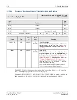
R/W
PB_RST
0
EEPROM
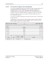
Master Decode Enable
Enables Master Decode when the Processor Bus arbiter is in
use — the Processor Bus Arbiter Enable bit, in the
Control and Status Register” on page 324
, is set. If MD_EN is
cleared, only the Processor Bus Address and Transaction
Type are used for transaction decode. If MD_EN is set, the
originating master is included in the transaction decode. A
transaction is claimed only if it originates from the master(s)
specified in
“Processor Bus Slave Image x Translation
0=Disable
1=Enable
BS[4:0]
R/W
PB_RST
0 EEPROM
Block Size
(4 Kbyte*2
BS
)
Specifies the size of the image, address lines compared and
address lines translated (see
).
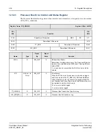
MODE
R/W
PB_RST
0
EEPROM
Image Mode
Determines if the image is used to generate Memory or IO
commands on PCI.
0 = Memory command generation
1 = I/O command generation or 4 byte memory read (see
DEST
R/W
PB_RST
0
EEPROM
Destination Bus
Selects the destination bus for the transaction.
0 = PCI 1 bus
1 = PCI-2 bus
Single PCI PowerSpan II: Reserved
PCI-1 Bus is the only destination.
MEM_IO
R/W
PB_RST
0
MEM_IO mode
PowerSpan II supports 4-byte reads. When this bit is set, the
Memory Read command to the corresponding image
generates the Memory Read command on the destination
PCI bus with a minimum 32 bit aligned 4-byte read.
The MODE bit and the MEM_IO bit work together to control
the size of the transaction (see
0 = Regular I/O mode
1 = Enables 1,2,3, or 4 byte memory reads on the PCI
bus(es)
Name
Type
Reset
By
Reset
State
Function


