12. Register Descriptions
299
PowerSpan II User Manual
80A1010_MA001_09
Integrated Device Technology
www.idt.com
12.5.28
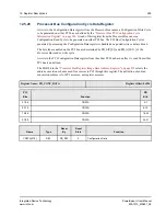
Processor Bus Configuration Cycle Data Register
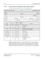
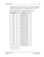
A write to the Configuration Data register from the Processor Bus causes a Configuration Write Cycle
to be generated on either PCI bus as defined by the
“Processor Bus PCI Configuration Cycle
Information Register” on page 296
. A read of this register from the Processor Bus causes a
Configuration Read Cycle to be generated on either PCI bus. The PCI Bus Configuration Cycles
generated by accessing the Configuration Data register is handled as a posted write or delayed read.
The byte lanes enabled on the PCI bus are determined by PB_SIZ[0:3] and PB_A[30:31] of the
Processor Bus read or write cycle.
A write to the PCI Configuration Data register from the either PCI bus has no effect. A read from either
PCI bus is undefined.
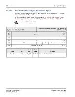
The END bit in the
“Processor Bus Register Image Base Address Register” on page 295
selects the
endian conversion scheme used for accesses to PCI through this register. The definition of endian
conversion scheme is for PCI accesses, not register accesses.
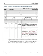
Register Name: PB_CONF_DATA
Register Offset: 0x294
PCI
Bits
Function
PB
Bits
31-24
CDATA
0-7
23-16
CDATA
8-15
15-08
CDATA
16-23
07-00
CDATA
24-31
Name
Type
Reset
By
Reset
State
Function
CDATA[31:0]
R/W
PB_RST
0
Configuration Data


