3. Processor Bus Interface
110
PowerSpan II User Manual
80A1010_MA001_09
Integrated Device Technology
www.idt.com
3.4.2.4
Cache Line Size
The PowerPC processors supported by PowerSpan II implement a 32-byte cache line size (8 words).
Cache wrap bursts are not generated because the PB master starts a burst transaction at a 32-byte
aligned address. For a transaction that is not 32-byte aligned, the PB master utilizes one or more single
beat or extended transaction size, to align to the cache line boundary, before generating the required
burst transaction or transactions.
3.4.2.5
Data Parity
Data Parity is enabled by setting the DP_EN bit in the Processor Bus Control and Status register (see
“Processor Bus Miscellaneous Control and Status Register” on page 304
). Even or odd parity can be
enabled by setting the PARITY bit on the Processor Bus Control and Status register.
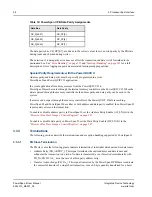
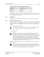
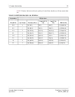
Parity generation and checking is provided for each byte of the data bus and for each data beat of the
data tenure. Data parity bit assignments are as defined in
.
The data parity bits, PB_DP[0:7], are driven to the correct values for even or odd parity by the PB
Master during writes. If checking is enabled (by setting the DP_EN bit) the data parity bits,
PB_DP[0:7], are checked by the PB Master during reads. The detection of a data parity error does not
affect the transaction, and data is still forwarded to the destination.
and
“Interrupt Handling” on page 145
for a full description of error
logging support and associated interrupt mapping options.
The PowerSpan II PB Master assumes all external slaves can accept burst transactions.
Table 25: PowerSpan II PB Data Parity Assignments
Data Bus
Data Parity
PB_D[0:7]
PB_DP[0]
PB_D[8:15]
PB_DP[1]
PB_D[16:23]
PB_DP[2]
PB_D[24:31]
PB_DP[3]
PB_D[32:39]
PB_DP[4]
PB_D[40:47]
PB_DP[5]
PB_D[48:55]
PB_DP[6]
PB_D[56:63]
PB_DP[7]


