


GD32E23x User Manual
261
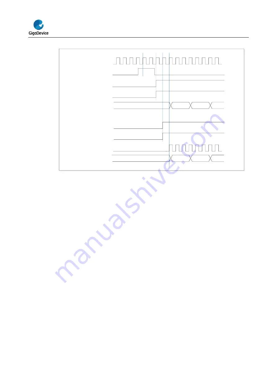
Figure 14-30
. Triggering TIMER0 and TIMER2 with TIMER2’s CI0 input
TIMER_CK
CNT_REG
CNT_REG
CI0
00
01
CEN
02
03
00
01
02
03
CNT_CK
TRGIF
CEN
TRGIF
TIMER2
TIMER0
Timer DMA mode
Timer DMA mode is the f
unction that configures timer’s register by DMA module. The relative
registers are TIMERx_DMACFG and TIMERx_DMATB.
Corresponding
DMA request bit
should be asserted to enable DMA request for internal interrupt event. TIMERx will send a
request to DMA when the interrupt event occurs. DMA is configured to M2P (memory to
peripheral) mode and the address of TIMERx_DMATB is configured to PADDR (peripheral
base address), then DMA will access the TIMERx_DMATB. In fact, TIMERx_DMATB
register is only a buffer, timer will map the TIMERx_DMATB to an internal register, appointed
by the field of DMATA in TIMERx_DMACFG. If the field of DMATC in TIMERx_DMACFG is 0
(1 transfer), the timer sends only one DMA request. While if TIMERx_DMATC is not 0, such
as 3 (4 transfers), th
en timer will send 3 more requests to DMA, and DMA will access timer’s
registers DMATA+0x4, DMATA+0x8 and DMATA+0xC at the next 3 accesses to
TIMERx_DMATB. In a word, one-time DMA internal interrupt event asserts, (DMATC+1)
times request will be sent by TIMERx.
If one more DMA request event occurs, TIMERx will repeat the process above.
Timer debug mode
When the Cortex
®
-M23 is halted, and the TIMERx_HOLD configuration bit in DBG_CTL0
register is set to 1, the TIMERx counter stops.


