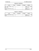


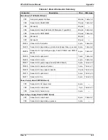
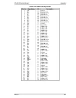


Table A-2. CN2 Pin Assignments (Continued)
Pin No.
Signal Name
I/O
Description
50
DQ24
I/O
Data bus bit 24
51
DQ9
I/O
Data bus bit 9
52
DQ25
I/O
Data bus bit 25
53
DQ10
I/O
Data bus bit 10
54
DQ26
I/O
Data bus bit 26
55
DQ11
I/O
Data bus bit 11
56
DQ27
I/O
Data bus bit 27
57
DQ12
I/O
Data bus bit 12
58
DQ28
I/O
Data bus bit 28
59
Vcc
—
+5 VDC
60
DQ29
I/O
Data bus bit 29
61
DQ13
I/O
Data bus bit 13
62
DQ30
I/O
Data bus bit 30
63
DQ14
I/O
Data bus bit 14
64
DQ31
I/O
Data bus bit 31
65
DQ14
I/O
Data bus bit 14
66
NC
—
Not connected
67
PO1
—
Not used
68
PO2
—
Not used
69
PO3
—
Not used
70
PO4
—
Not used
71
NC
—
Not connected
72
Vss
—
Ground
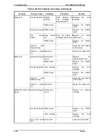
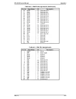
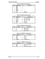
Table A-3. CN4 Pin Assignments
Pin No.
Signal Name
I/O
Description
1
PCLK
O
Clock
2
RST
O
Reset signal
3
GND
—
Ground
4
GND
—
Ground
5
GND
—
Ground
6
GND
—
Ground
7
DB0
I/O
Data bus bit 0
8
DB1
I/O
Data bus bit 1
9
DB2
I/O
Data bus bit 2
10
DB3
I/O
Data bus bit 3
11
DB4
I/O
Data bus bit 4
12
DB5
I/O
Data bus bit 5
13
DB6
I/O
Data bus bit 6
14
DB7
I/O
Data bus bit 7
15
AB0
O
Address bus bit 0
16
AB1
O
Address bus bit 1
17
AB2
O
Address bus bit 2
18
AB3
O
Address bus bit 3
19
AB4
O
Address bus bit 4
20
CS
O
Select signal
EPL-5500 Service Manual
Appendix
Rev. A
A-5
Summary of Contents for EPL-5500
Page 1: ...EPSON TERMINAL PRINTER EPL 5500 SERVICE MANUAL EPSON 4005431 ...
Page 2: ... ii ...
Page 12: ...Rev A 1 iii ...
Page 62: ...EPL 5500 Service Manual Operating Principles Rev B 2 11 ...
Page 122: ...6 ii Rev A ...
Page 125: ...EPL 5500 Service Manual Maintenance Rev B 6 3 ...
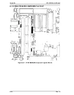
Page 142: ...Figure A 8 C169 MAIN B Component Layout Rear EPL 5500 Service Manual Appendix Rev A A 17 ...
Page 144: ......
Page 145: ...EPSON ...