


H A R D W A R E
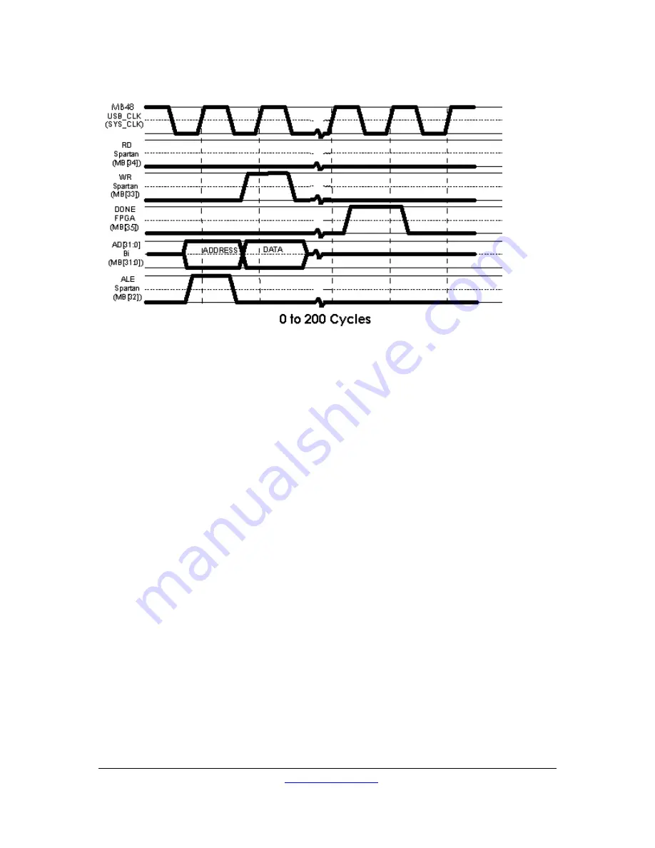
When the Spartan asserts the “WR” signal, the FPGA should register the data on the AD bus.
Sometime after this, the FPGA should assert the DONE signal. This will allow the Spartan to
begin more transactions. The FPGA may delay this for up to 256 clock cycles before a timeout
is recorded and the transaction is cancelled.
Main bus can be controlled from the USB Controller program. (Read and write single addresses,
or to/from files) It can also be written from the main.txt configuration method. The main.txt
syntax is
MAIN BUS 0x<address> 0x<data>
Where <address> and <data> are 8-digit (32-bit) hexadecimal numbers.
18.3.1
Conventional Memory map
By convention, FPGAs on the main bus interface are assigned address ranges. Assigning address
ranges is required because the “FPGA sourced” signals (DONE) need to be driven by only one
FPGA at a time.
The convention that Dini Group uses is to reserve the upper four bits in the address as an
FPGA-select address. The address range (hex)
0x00000000 – 0x0FFFFFFF is reserved for FPGA A
0x10000000 – 0x1FFFFFFF is reserved for FPGA B
and so on.
The user need not follow this convention, but unless you really need 32-bit addresses, we
recommend using it. Only one FPGA has “control” of the DONE signal. If the last address
latched by ALE was not for a given FPGA, it should tri-state the output. Before tri-stating any
DN9002K10PCI User Guide
www.dinigroup.com
110
Summary of Contents for DN9002K10PCI
Page 1: ...LOGIC Emulation Source UserGuide DN9002K10PCI ...
Page 3: ......
Page 34: ......
Page 46: ...C O N T R O L L E R S O F T W A R E DN9002K10PCI User Guide www dinigroup com 36 ...
Page 150: ......


