Major Chips Description
2-21
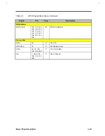
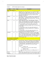
Table 2-3
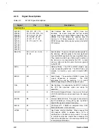
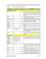
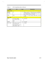
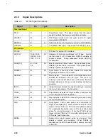
M1523 Signal Descriptions (continued)
Signal
Pin
Type
Description
ISA Interface
SMEMRJ / LMEGJ
176
O
ISA System Memory Read. When the internal RTC is
enabled, this signal indicates that the memory read cycle
is for an address below 1-MB address. Otherwise, this pin
only indicates an address below 1M byte.
SMEMWJ / RTCAS
174
O
ISA System Memory Write. When the internal RTC is
enabled, this signal indicates that the memory write cycle
is for an address below 1-MB address. Otherwise, this pin
is used as RTC address strobe.
DREQJ[7:5]
DREQJ[3:0]
38, 34, 30,
186, 166, 189,
25
I
DMA Request Signals. These are DMA request input
signals.
DACKJ[7:5] /
DAK_SEL[2:0]
DACKJ[3] / PCSJ,
DACKJ[2] /
DACKOJDACKJ[1],
DACKJ[0]
36,32,
28,
184,
204,
48,
47
O
I/O
O
When DACKJ polling mode is disabled, these pins are
DACKJ[7:5,3:0](O). Otherwise, these pins are
DAK_SEL[2:0](O) connect to external MUX select inputs,
PCSJ(O) programmable chip select, and DACKOJ(O)
connected to external MUX chip enable.
TC
206
O
DMA End of Process. Hardware setting options:
Pulled low: Support external I/O APIC mode
Pulled high: Not support external I/O APIC
REFSHJ
191
I/O
ISA Refresh Cycle. This signal is input during ISA master
cycles, but an output during other cycles.
Timer
SPKR
43
O
Speaker Output. Hardware setting options:
Pulled low: Enable Internal KBC
Pulled high: Disable Internal KBC
Miscellaneous
SPLED
44
O
Speed LED Output. Hardware setting options:
Pulled low:
Enable DMA DACKJ[7:5,3:0]
polling mode
Pulled high:
Disable DMA DACKJ[7:5;3:0]
polling mode
ROMCSJ
158
O
ROM and RTC Chip Select. This signal must be pulled
high for normal operation.
XDIR
159
O
X-bus Direction Control. Hardware setting option: must be
pulled high.
KBINH/ IRQ1
151
I
KB Inhibit Input when the internal KBC is enabled.
IRQ1 Input when the internal KBC is disabled
KBCLK/ KBCSJ
152
I/O
KB interface CLK when the internal KBC is enabled.
KB Chip Select when the internal KBC is disabled
KBDATA
153
O
KB interface Data when the internal KBC is enabled.
Summary of Contents for Extensa 61X
Page 6: ...vi ...
Page 26: ...1 8 Service Guide Figure 1 5 Main Board Layout Bottom Side ...
Page 49: ...System Introduction 1 31 1 5 1 3 Power Management Figure 1 14 Power Management Block Diagram ...
Page 55: ...System Introduction 1 37 1 6 System Block Diagram Figure 1 15 System Block Diagram ...
Page 64: ...Major Chips Description 2 7 2 2 5 Pin Diagram Figure 2 4 M1521 Pin Diagram ...
Page 99: ...2 42 Service Guide 2 5 3 Pin Diagram Figure 2 10 C T 65550 Pin Diagram ...
Page 117: ...2 60 Service Guide Figure 2 12 Functional block diagram CardBus Card Interface ...
Page 119: ...2 62 Service Guide Figure 2 14 PCI to CardBus terminal assignments ...
Page 135: ...2 78 Service Guide 2 7 3 Pin Diagram Figure 2 16 NS87336VJG Pin Diagram ...
Page 145: ...2 88 Service Guide 2 8 2 Pin Diagram Figure 2 17 YMF715 Block Diagram ...
Page 185: ...Disassembly and Unit Replacement 4 5 Figure 4 3 Disassembly Sequence Flowchart ...
Page 209: ...B 2 Service Guide ...
Page 210: ...Exploded View Diagram B 3 ...


