2-32
Service Guide
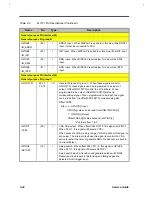
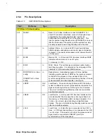
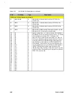
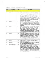
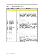
Table 2-4
M7101 Pin Descriptions (Continued)
Name
No.
Type
Description
General purpose I/O interface(24)
General purpose I/O group B
GPIOB3
/IN_BRDYJ
(84)
I
BRDYJ Input. When DISPLAY is pulled low, this pin will be BRDYJ
input. It must be connected to CPU.
GPIOB2
/IN_INIT
(83)
I
INIT Input. When DISPLAY is pulled low, this pin will be INIT input.
GPIOB1
/IN_SMIJ
(82)
I
SMIJ Input. When DISPLAY is pulled low, this pin will be SMIJ
input.
GPIOB0
/IN_INTR
(81)
I
SMIJ Input. When DISPLAY is pulled low, this pin will be INTR
input.
General purpose I/O interface(24)
General purpose I/O group C
GPIOC[7:0]
80-77,
75-72
I/O
General Purpose I/O group C. When these signals are set to
GPIOC[7:0], these signals can be programmed to be input or
output. Offset 0DDh D[7:0] control the I/O attribute. When
programmed to be output, offset 0DCh D[7:0] will set to
corresponding signal. When programmed to be input, the signal
can be read from the Offset 0DCh D[7:0] corresponding bits.
Offset 0DDh
D[n] = 0 : GPIOC[n]=input
GPIOC[n] value can be read from Offset 0DCh D[n]
1 : GPIOC[n]=Output
Offset 0DAh D[n] value will send to GPIOC[n]
"n" value is from 7 to 0
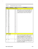
GPIOC7
/VCSJ
(80)
I
VGA Chip select. When offset 0F6h D12=0, this signal is GPIOC7.
When D12=1, this signal will become VCSJ.
When access to VGA memory range, VGA chip will set this signal to
active low. The internal circuit use this signal to monitor the VGA
active to restart the timer or generate SMIJ. No debounce is built in.
Low level detect.
GPIOC6
/SETUPJ
(79)
I
Setup switch. When offset 0F6h D11=0, this signal is GPIOC6.
When D11=1, this signal will become SETUPJ.
Setup switch input. A transition will generate setup switch SMIJ.
Debounce circuit is built in. Both rising and falling edges are
detected. Smith-trigger input.
Summary of Contents for Extensa 61X
Page 6: ...vi ...
Page 26: ...1 8 Service Guide Figure 1 5 Main Board Layout Bottom Side ...
Page 49: ...System Introduction 1 31 1 5 1 3 Power Management Figure 1 14 Power Management Block Diagram ...
Page 55: ...System Introduction 1 37 1 6 System Block Diagram Figure 1 15 System Block Diagram ...
Page 64: ...Major Chips Description 2 7 2 2 5 Pin Diagram Figure 2 4 M1521 Pin Diagram ...
Page 99: ...2 42 Service Guide 2 5 3 Pin Diagram Figure 2 10 C T 65550 Pin Diagram ...
Page 117: ...2 60 Service Guide Figure 2 12 Functional block diagram CardBus Card Interface ...
Page 119: ...2 62 Service Guide Figure 2 14 PCI to CardBus terminal assignments ...
Page 135: ...2 78 Service Guide 2 7 3 Pin Diagram Figure 2 16 NS87336VJG Pin Diagram ...
Page 145: ...2 88 Service Guide 2 8 2 Pin Diagram Figure 2 17 YMF715 Block Diagram ...
Page 185: ...Disassembly and Unit Replacement 4 5 Figure 4 3 Disassembly Sequence Flowchart ...
Page 209: ...B 2 Service Guide ...
Page 210: ...Exploded View Diagram B 3 ...

