2-2
Service Guide
2.2
ALI M1521
The ALADDIN-III consists of two chips, ALI M1521 and M1523 to give a 586 class system the
complete solution with the most up-to-date feature and architecture for the new
multimedia/multithreading operating system. It utilizes the BGA package to improve the AC
characterization, resolves system bottleneck and make the system manufacturing easier. The
ALADDIN-III gives a highly-integrated system solution and a most up-to-date system architecture
including the UMA, ECC, PBSRAM, SDRAM/BEDO, and multi-bus with highly efficient, deep FIFO
between the buses, such as the HOST/PCI/ISA dedicated IDE bus.
The M1521 provides a complete integrated solution for the system controller and data path
components in a Pentium-based system. It provides 64-bit CPU bus interface, 32-bit PCI bus
interface, 64/72 DRAM data bus with ECC or parity, secondary cache interface including pipeline
burst SRAM or asynchronous SRAM, PCI master to DRAM interface, four PCI master arbiters, and
a UMA arbiter. The M1521 bus interfaces are designed to interface with 3V and 5V buses. It
directly connects to 3V CPU bus, 3V or 5V tag, 3V or 5V DRAM bus, and 5V PCI bus.
2.2.1
Features
•
Supports all Intel/Cyrix/AMD 586-class processors (with host bus of 66 MHz, 60 MHz and
50 MHz at 3V)
•
supports M1/K5/Dakota CPUs
•
supports linear wrap mode for M1
•
Supports asynchronous/pipeline-burst SRAM
•
Write-back/dynamic write-back cache policy
•
Built-in 8K*2 bit SRAM for MESI protocol to cost and enhance performance
•
Cacheable memory up to 512MB with 11-bit tag SRAM
•
Supports 3V/5V SRAMs for tag address
•
Supports FPM/EDO/BEDO/SDRAM DRAMs
•
RAS lines
•
64-bit data path to memory
•
Symmetrical/asymmetrical DRAMs
•
3V or 5V DRAMs
•
Duplicated MA[1:0] driving pins for burst access
•
No buffer needed for RASJ and CASJ and MA[1:0]
•
CBR and RAS-only refresh
•
Supports 64M-bit (16M*4, 8M*8, 4M*16) technology DRAMs
•
Supports programmable-strength MA buffer
•
Supports error checking and correction (ECC) and parity for DRAM
•
Supports the most flexible six 32-bit populated banks of DRAM (to spare 12MB for
Windows 95)
•
Supports SIMM and DIMM
Summary of Contents for Extensa 61X
Page 6: ...vi ...
Page 26: ...1 8 Service Guide Figure 1 5 Main Board Layout Bottom Side ...
Page 49: ...System Introduction 1 31 1 5 1 3 Power Management Figure 1 14 Power Management Block Diagram ...
Page 55: ...System Introduction 1 37 1 6 System Block Diagram Figure 1 15 System Block Diagram ...
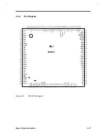
Page 64: ...Major Chips Description 2 7 2 2 5 Pin Diagram Figure 2 4 M1521 Pin Diagram ...
Page 99: ...2 42 Service Guide 2 5 3 Pin Diagram Figure 2 10 C T 65550 Pin Diagram ...
Page 117: ...2 60 Service Guide Figure 2 12 Functional block diagram CardBus Card Interface ...
Page 119: ...2 62 Service Guide Figure 2 14 PCI to CardBus terminal assignments ...
Page 135: ...2 78 Service Guide 2 7 3 Pin Diagram Figure 2 16 NS87336VJG Pin Diagram ...
Page 145: ...2 88 Service Guide 2 8 2 Pin Diagram Figure 2 17 YMF715 Block Diagram ...
Page 185: ...Disassembly and Unit Replacement 4 5 Figure 4 3 Disassembly Sequence Flowchart ...
Page 209: ...B 2 Service Guide ...
Page 210: ...Exploded View Diagram B 3 ...


