Major Chips Description
2-83
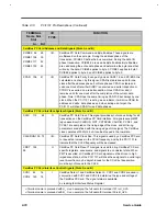
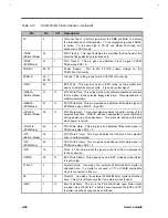
Table 2-14
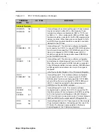
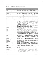
NS87336VJG Pin Descriptions (continued)
Pin
No.
I/O
Description
IORCHDY
51
O
I/O Channel Ready. When IORCHDY is driven low, the EPP extends
the host cycle.
IRQ3, 4
IRQ5-7
IRQ9-11
IRQ12, 15
(PnP Mode)
99, 98
96-94,
55-57,
66, 58
I/O
Interrupt 3, 4, 5, 6, 7, 9, 10, 11, 12, and 15. This pin can be a totem-
pole output or an open-drain output. The interrupt can be sourced by
one of the following: UART1 and/or UART2, parallel port, FDC,
SIRQI1 pin, SIRQI2 pin or SIRQI3 pin.
IRQ5 is multiplexed with ADRATE0.
IRQ12 is multiplexed with /DSR2 and IRRX2.
IRQ15 is multiplexed with SIRQI1.
IRQ3, 4
(Legacy Mode)
99, 98
O
Interrupt 3 and 4. These are active high interrupts associated with
the serial ports. IRQ3 presents the signal if the serial channel ahs
been designated as COM2 or COM4. IRQ4 presents the signal if the
serial port is designated as COM1 or COM3. The interrupt is reset
low (inactive ) after the appropriate interrupt service routine is
executed.
IRQ5
(Legacy Mode)
96
I/O
Interrupt 5. Active high output that indicates a parallel port interrupt.
When enabled, this pin follows the /ACK signal input. When it is noe
enabled, this signal is tri-state. This pin ia I/O only when ECP is
enabled, and IRQ5 is configured.
IRQ6
(Legacy Mode)
95
O
Interrupt 6. Active high output to signal the completion of the
execution phase for certain FDC commands. Also used to signal
when a data transfer is ready during a non-DMA operation.
IRQ7
(Legacy Mode)
94
I/O
Interrupt 7. Active high output that indicates a parallel port interrupt.
When enabled, this signal follows the /ACK signal intput. When it is
not enabled, this signal is tri-state. This pin is I/O only when ECP is
enabled, and IRQ7 is configured.
IRRX1
IRRX2
65, 66
I
IrDA or SHARP- Infrared Receive. One of these pins is the infrared
serial data input.
IRRX1 is multiplexed with SIN2.
IRRX2 is multiplexed with /DSR2 and IRQ12.
IRTX
63
O
Infrared Transmit. Infrared serial data output. Software configuration
selects either IrDA or Sharp-IR protocol.
This pin is multiplexed with SOUT2/BOUT/CFG0.
MR
100
I
Master Reset. Active high output that resets the controller to the idle
state and resets all disk interface outputs to their inactive states. The
DOR, DSR, CCR, Mode command, Configure command, and Lock
command parameters are cleared to their default values. The
Specify command parameters are not affected
Summary of Contents for Extensa 61X
Page 6: ...vi ...
Page 26: ...1 8 Service Guide Figure 1 5 Main Board Layout Bottom Side ...
Page 49: ...System Introduction 1 31 1 5 1 3 Power Management Figure 1 14 Power Management Block Diagram ...
Page 55: ...System Introduction 1 37 1 6 System Block Diagram Figure 1 15 System Block Diagram ...
Page 64: ...Major Chips Description 2 7 2 2 5 Pin Diagram Figure 2 4 M1521 Pin Diagram ...
Page 99: ...2 42 Service Guide 2 5 3 Pin Diagram Figure 2 10 C T 65550 Pin Diagram ...
Page 117: ...2 60 Service Guide Figure 2 12 Functional block diagram CardBus Card Interface ...
Page 119: ...2 62 Service Guide Figure 2 14 PCI to CardBus terminal assignments ...
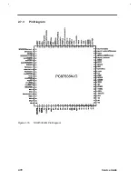
Page 135: ...2 78 Service Guide 2 7 3 Pin Diagram Figure 2 16 NS87336VJG Pin Diagram ...
Page 145: ...2 88 Service Guide 2 8 2 Pin Diagram Figure 2 17 YMF715 Block Diagram ...
Page 185: ...Disassembly and Unit Replacement 4 5 Figure 4 3 Disassembly Sequence Flowchart ...
Page 209: ...B 2 Service Guide ...
Page 210: ...Exploded View Diagram B 3 ...


