System Introduction
1-
5
1.1.4
System Specifications Overview
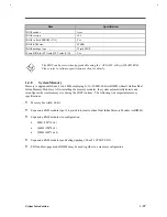
Table 1-3
System Specifications
Item
Standard
Optional
Microprocessor
Intel Pentium™ processor
(Intel P54CSLM 120/133/150 MHz)
Intel P55CLM - 133/150 with MMX
System memory
8MB / 16MB
Dual 64-bit memory banks
Expandable to 64MB using 8, 16 and 32MB
soDIMMs
Flash ROM BIOS
256KB
Data storage devices
CD-ROM model
FDD model
Removable 12.5mm, 2.5-inch, 1.0GB
Enhanced-IDE hard disk
Internal 15mm, 5.25-inch high-speed
CD-ROM drive
Internal 3.5-inch, 1.44MB floppy drive
1
+
GB Enhanced-IDE hard disk drive
External 3.5-inch, 1.44MB diskette drive
Display
DualScan STN or TFT active matrix,
800x600, 256 colors (SVGA)
Up to 1024x768, 256-color ultra-VGA
monitor
LCD projection panel
Video
PCI local bus video with graphics
accelerator and 1MB video RAM
Audio
16-bit stereo audio; built-in dual
speakers; separate audio ports
Keyboard and pointing
device
84-/85-/88-key with Windows 95 keys
Touchpad (centrally-located on palmrest)
101-/102-key, PS/2-compatible keyboard or
17-key numeric keypad
External serial or PS/2 mouse or similar
pointing device
I/O ports
One 9-pin RS-232 serial port
(UART16550-compatible)
One 25-pin parallel port
(EPP/ECP-compliant)
One 15-pin CRT port
One 6-pin PS/2 keypad/ keyboard/mouse
connector
One type III or two type II PC Card
slot(s) with ZV port support
One external FDD port
Serial mouse, printer or other serial devices
Parallel printer or other parallel devices
Up to a 1024x768, 256-color
ultra-VGA monitor
17-key numeric keypad, PS/2 keyboard or
mouse
LAN card or other PC cards
External diskette drive
Summary of Contents for Extensa 61X
Page 6: ...vi ...
Page 26: ...1 8 Service Guide Figure 1 5 Main Board Layout Bottom Side ...
Page 49: ...System Introduction 1 31 1 5 1 3 Power Management Figure 1 14 Power Management Block Diagram ...
Page 55: ...System Introduction 1 37 1 6 System Block Diagram Figure 1 15 System Block Diagram ...
Page 64: ...Major Chips Description 2 7 2 2 5 Pin Diagram Figure 2 4 M1521 Pin Diagram ...
Page 99: ...2 42 Service Guide 2 5 3 Pin Diagram Figure 2 10 C T 65550 Pin Diagram ...
Page 117: ...2 60 Service Guide Figure 2 12 Functional block diagram CardBus Card Interface ...
Page 119: ...2 62 Service Guide Figure 2 14 PCI to CardBus terminal assignments ...
Page 135: ...2 78 Service Guide 2 7 3 Pin Diagram Figure 2 16 NS87336VJG Pin Diagram ...
Page 145: ...2 88 Service Guide 2 8 2 Pin Diagram Figure 2 17 YMF715 Block Diagram ...
Page 185: ...Disassembly and Unit Replacement 4 5 Figure 4 3 Disassembly Sequence Flowchart ...
Page 209: ...B 2 Service Guide ...
Page 210: ...Exploded View Diagram B 3 ...

