Major Chips Description
2-49
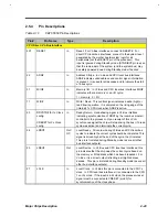
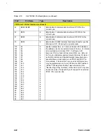
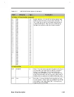
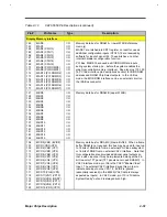
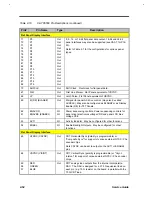
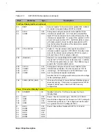
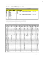
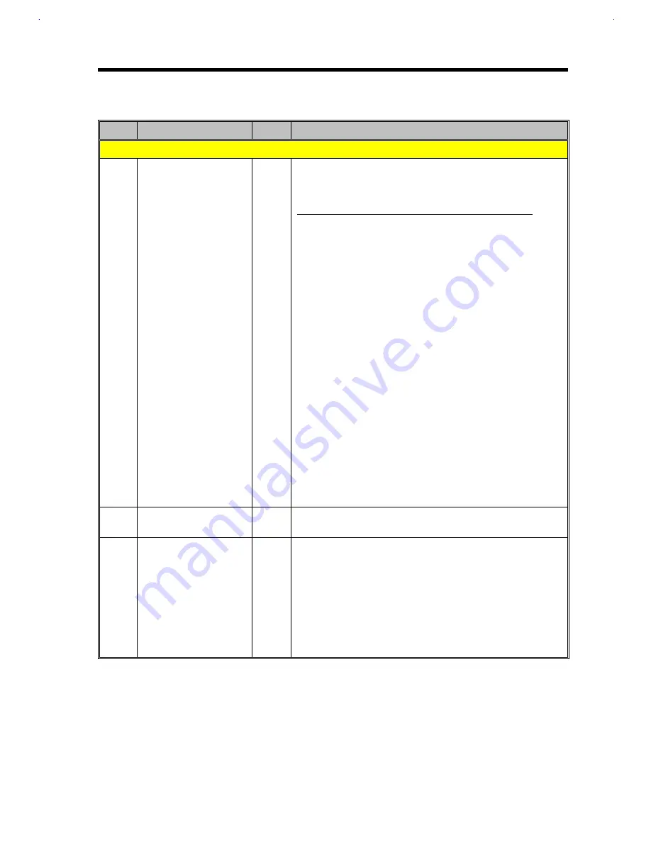
Table 2-10
C&T 65550 Pin Descriptions (continued)
Pin#
Pin Name
Type
Description
PCI Bus Interface (continued)
43
32
21
10
C/BE0#
C/BE1#
C/BE2#
C/BE3#
In
In
In
In
Bus Command / Byte Enables. During the address phase. of
a bus transaction, these pins define the bus command see
list below:
C/BE3-0 Command Type 65550
0000
Interrupt Acknowledge
0001
Special Cycle
0010
I/O Read
Y
0011
I/O Write
Y
0100
-reserved-
0101
-reserved-
0110
Memory Read
Y
0111
Memory Write
Y
1000
-reserved-
1001
-reserved-
1010
Configuration Read
Y
1011
Configuration Write
Y
1100
Memory Read Multiple
1101
Dual Address Cycle
1110
Memory Read Line
1111
Memory Read & Invalidate
During the data phase, these pins are byte enables that
determine which byte lanes carry meaningful data:
byte 0 corresponds to AD0-7,
byte 1 corresponds to 8-15,
byte 2 corresponds to 16-23,
byte 3 corresponds to 24-31
11
IDSEL
Initialization. Device Select. Used as a chip select during
configuration read and write transactions.
145
146
147
148
149
150
151
152
153
AA0
AA1
AA2
AA3
AA4
AA5
AA6
AA7
AA8
I/O
I/O
I/O
I/O
I/O
I/O
I/O
I/O
I/O
Address bus for DRAMs A and B.
Summary of Contents for Extensa 61X
Page 6: ...vi ...
Page 26: ...1 8 Service Guide Figure 1 5 Main Board Layout Bottom Side ...
Page 49: ...System Introduction 1 31 1 5 1 3 Power Management Figure 1 14 Power Management Block Diagram ...
Page 55: ...System Introduction 1 37 1 6 System Block Diagram Figure 1 15 System Block Diagram ...
Page 64: ...Major Chips Description 2 7 2 2 5 Pin Diagram Figure 2 4 M1521 Pin Diagram ...
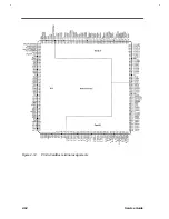
Page 99: ...2 42 Service Guide 2 5 3 Pin Diagram Figure 2 10 C T 65550 Pin Diagram ...
Page 117: ...2 60 Service Guide Figure 2 12 Functional block diagram CardBus Card Interface ...
Page 119: ...2 62 Service Guide Figure 2 14 PCI to CardBus terminal assignments ...
Page 135: ...2 78 Service Guide 2 7 3 Pin Diagram Figure 2 16 NS87336VJG Pin Diagram ...
Page 145: ...2 88 Service Guide 2 8 2 Pin Diagram Figure 2 17 YMF715 Block Diagram ...
Page 185: ...Disassembly and Unit Replacement 4 5 Figure 4 3 Disassembly Sequence Flowchart ...
Page 209: ...B 2 Service Guide ...
Page 210: ...Exploded View Diagram B 3 ...


