ZEISS
5 Commissioning and First Operating Steps | 5.7 Finding Appropriate Detector Settings
5.7.11 Setting up the SCD Detector
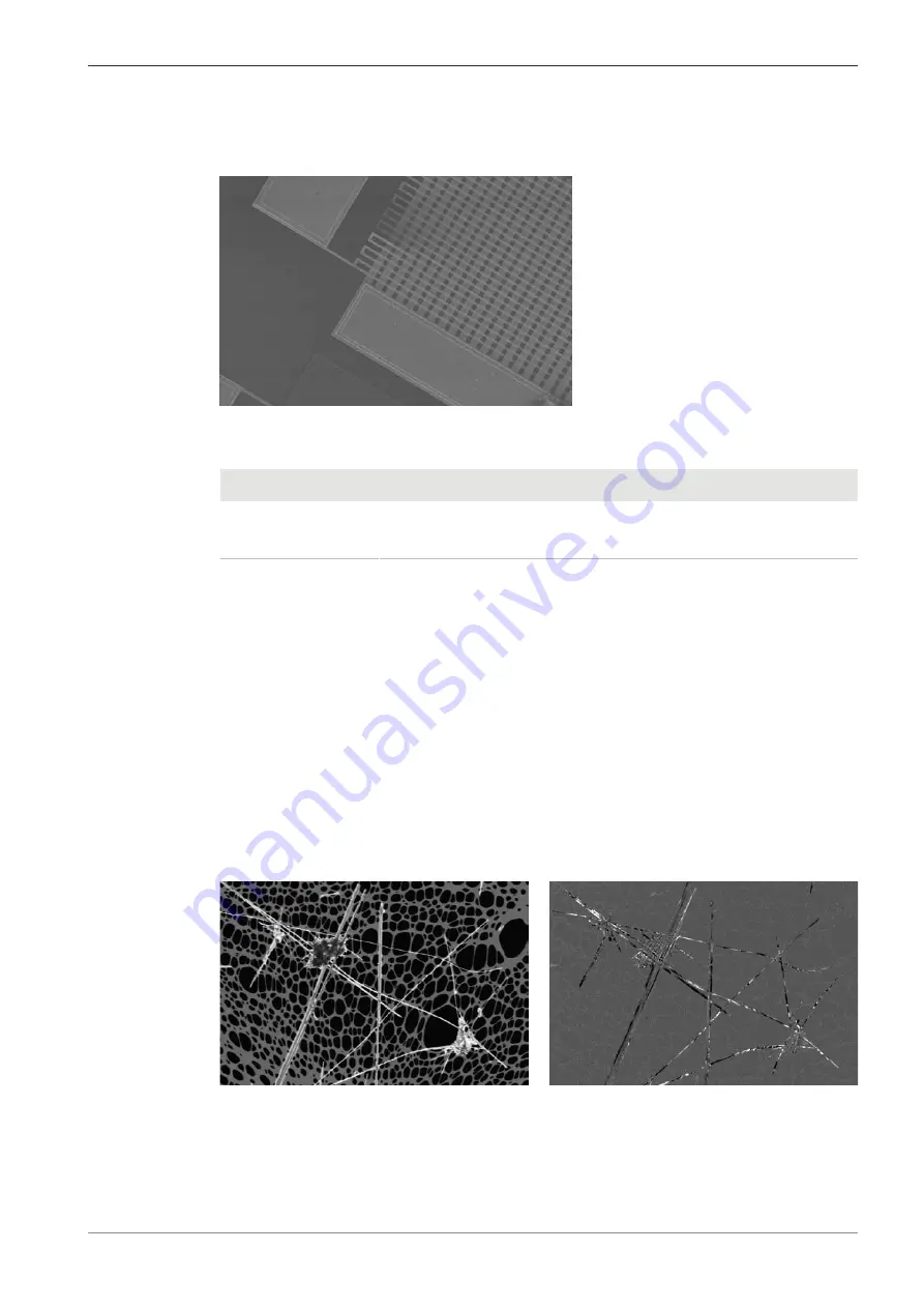
The SCD detects the current absorbed in the specimen. A highly sensitive amplifier is connected to
the sample, measuring the sum of incoming PEs and outgoing SEs and BSEs for each image pixel.
Fig. 48: Silicon chip
The following settings are recommended for the SCD detector:
Settings
10–30 kV
5–10 mm
Scanspeed: 8 and higher
Primary current: appr. 1 nA
Procedure
1. In the GeminiSEM Control panel, select the Imaging tab.
2. From the
Signal A
drop-down list, select
SCD
.
3. Adjust the EHT, working distance (WD), scan speed and primary current according to the
suggestions in the table in order to optimize the image.
5.7.12 Setting up the aSTEM Detector
The aSTEM detector is used for compositional imaging or topographical imaging of ultrathin spec-
imens. The aSTEM detector is available either with one video output channel (aSTEM1) or with
four video output channels (aSTEM4). The aSTEM detector is optionally available.
The aSTEM detector is equipped with several separate diode segments. The signals of the seg-
ments can individually be added to or subtracted from the output signal in order to allow differ-
ent STEM imaging modes, e.g. bright field (BF) or oriented dark field (ODF). The most commonly
used STEM imaging modes are predefined and can be selected from a drop-down menu in the
STEM Control
panel.
Fig. 49: Asbestos, oriented darkfield (ODF) image captured with an
image showing real information about bending and lattice defects within each fiber (right).
Instruction Manual ZEISS GeminiSEM series | en-US | Rev. 2 | 349500-8138-000
101


