Design Guide
89
Hub Interface
7.2.4
Hub Interface 2.0 Decoupling Guidelines
To improve I/O power delivery, use two 0.1 µF capacitors per component (i.e., MCH, P64H2).
These capacitors should be placed within 150 mils of each package, adjacent to the rows that
contain the hub interface. If the layout allows, wide metal fingers running on the VSS side of the
board should connect the VCC1.8/VCC1.2 side of the capacitors to the VCC1.8/VCC1.2 power
pins. Similarly, if layout allows, metal fingers running on the VCC1.8/VCC1.2 side of the board
should connect the ground side of the capacitors to the VSS power pins.
7.2.5
Unused Hub Interface 2.0 Interfaces
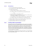
Terminate unused Hub Interface 2.0 interfaces as described below:
•
All hub interface data and strobe signals can be left as no connects.
•
HIVREF and HISWNG must remain connected to the reference voltage divider circuits (refer
to
). RCOMP must be pulled up to 1.2 V.
7.3
Hub Interface 1.5 Implementation
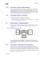
The Hub Interface 1.5 signals HI[7:0] are associated with HI_STBS/HI_STBF. For those familiar
with the Hub Interface 1.0 mode, HI_STBF and HI_STBS are called HI_STB# and HI_STB,
respectively.
This section documents the routing guidelines for the Hub Interface 1.5 that is responsible for
connecting the MCH to the ICH3-S. Hub Interface 1.5 supports parallel termination mode only,
therefore the DPRSLPVR pin on the ICH3-S must be left as No Connect (NC); this signal has an
internal pull-down.
7.3.1
Hub Interface 1.5 High-Speed Routing Guidelines
The MCH and ICH3-S ball assignments are optimized to simplify the hub interface routing
between these devices. Route the hub interface signals directly from the MCH to ICH3-S with all
signals referenced to ground. Keep layer transitions to a minimum. If a layer change is required,
use only two vias per net, and keep all data signals and associated strobe signals on the same layer.
The Hub Interface 1.5 signal groups are listed in
. The general routing guidelines for the
Hub Interface 1.5 signals are given in
Figure 7-7. 8-Bit Hub Interface 1.5 Routing
Intel
®
ICH3-S
MCH
CLK
Synthesizer
CLK66
CLK66
HI[11:0]
HI_STBS
HI_STBF
Содержание Xeon
Страница 24: ...Introduction 24 Design Guide This page is intentionally left blank ...
Страница 30: ...Component Quadrant Layout 30 Design Guide This page is intentionally left blank ...
Страница 34: ...Platform Stack Up and Component Placement Overview 34 Design Guide This page is intentionally left blank ...
Страница 52: ...Platform Clock Routing Guidelines 52 Design Guide This page is intentionally left blank ...
Страница 66: ...System Bus Routing Guidelines 66 Design Guide This page is intentionally left blank ...
Страница 118: ...Intel 82870P2 P64H2 118 Design Guide This page is intentionally left blank ...
Страница 146: ...I O Controller Hub 146 Design Guide This page is intentionally left blank ...
Страница 148: ...Debug Port 148 Design Guide This page is intentionally left blank ...
Страница 210: ...Schematic Checklist 210 Design Guide This page is intentionally left blank ...
Страница 220: ...Layout Checklist 220 Design Guide This page is intentionally left blank ...
Страница 222: ...Schematics 222 Design Guide This page is intentionally left blank ...


