I/O Controller Hub
136
Design Guide
9.7.1.2
Signal Routing and Layout
Route the LCI signals carefully on the motherboard to meet the timing and signal quality
requirements of this interface specification. The board designer should simulate the board routing
to verify that the specifications are met for flight times and skews due to trace mismatch and
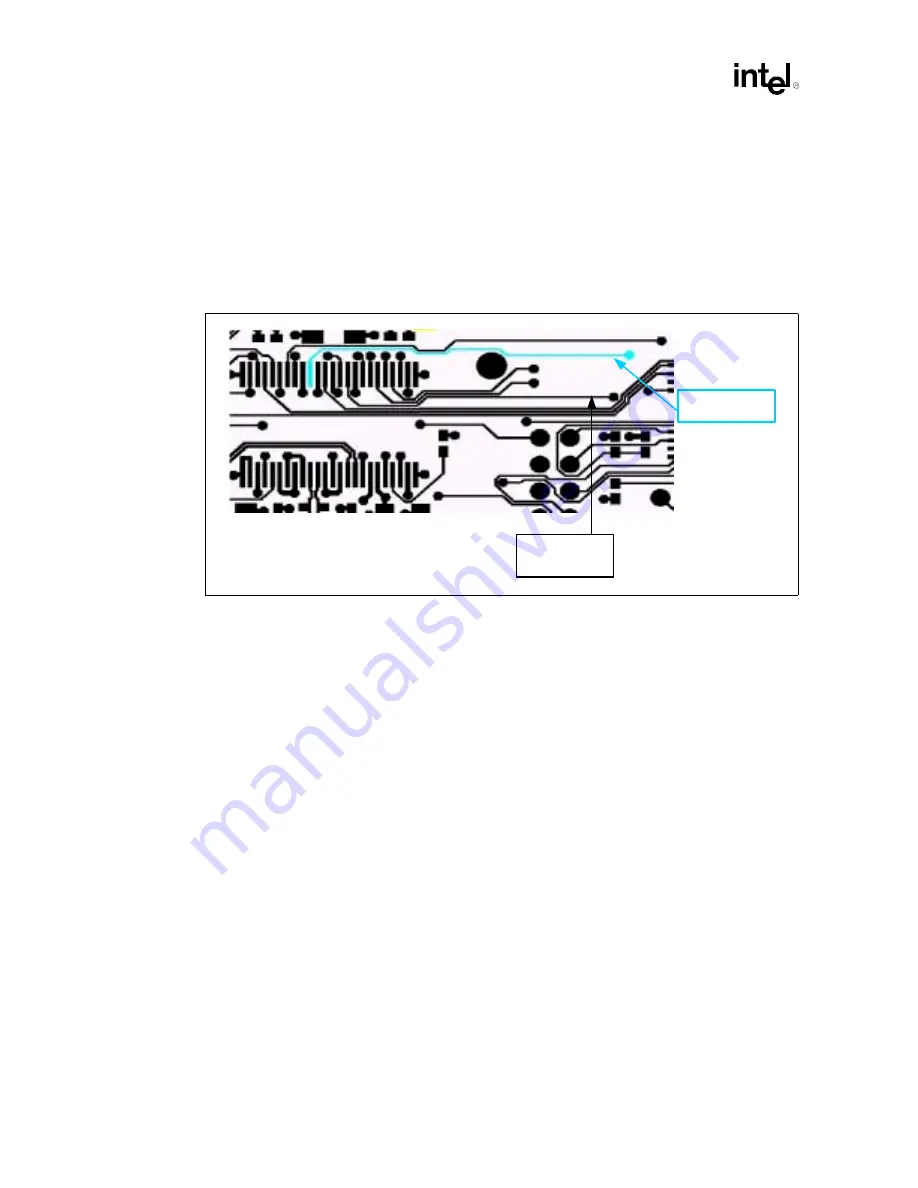
crosstalk. On the motherboard, the length of each data trace should be either equal in length to the
LAN_CLK trace, or up to 0.5" shorter than the LAN_CLK trace. (LAN_CLK should always be the
longest motherboard trace in each group.)
9.7.1.3
Crosstalk Consideration
Noise due to crosstalk must be carefully controlled to a minimum. Crosstalk is the key cause of
timing skews and is the largest part of the tRMATCH skew parameter. tRMATCH is the sum of the
trace length mismatch between LAN_CLK and the LAN data signals. To meet this requirement on
the board, the length of each data trace must be either equal to or up to 0.5 inch shorter than the
LAN_CLK trace. Maintaining at least 100 mils of spacing should minimize noise due to crosstalk
from non-LCI signals.
9.7.1.4
Impedances
The motherboard impedances should be controlled to minimize the impact of any mismatch
between the motherboard and the add-in card. An impedance of 60
Ω
± 15% is strongly
recommended; otherwise, signal integrity requirements may be violated.
9.7.1.5
Line Termination
Line termination mechanisms are not specified for the LAN Connect Interface. Slew rate
controlled output buffers achieve acceptable signal integrity by controlling signal reflection, over/
undershoot, and ringback. A 33
Ω
series resistor can be installed at the driver side of the interface
should the developer have concerns about over/undershoot. Note that the receiver must allow for
any drive strength and board impedance characteristic within the specified ranges.
Figure 9-16. LAN_CLK Routing Example
LAN_CLK
LAN_RXD0
Содержание Xeon
Страница 24: ...Introduction 24 Design Guide This page is intentionally left blank ...
Страница 30: ...Component Quadrant Layout 30 Design Guide This page is intentionally left blank ...
Страница 34: ...Platform Stack Up and Component Placement Overview 34 Design Guide This page is intentionally left blank ...
Страница 52: ...Platform Clock Routing Guidelines 52 Design Guide This page is intentionally left blank ...
Страница 66: ...System Bus Routing Guidelines 66 Design Guide This page is intentionally left blank ...
Страница 118: ...Intel 82870P2 P64H2 118 Design Guide This page is intentionally left blank ...
Страница 146: ...I O Controller Hub 146 Design Guide This page is intentionally left blank ...
Страница 148: ...Debug Port 148 Design Guide This page is intentionally left blank ...
Страница 210: ...Schematic Checklist 210 Design Guide This page is intentionally left blank ...
Страница 220: ...Layout Checklist 220 Design Guide This page is intentionally left blank ...
Страница 222: ...Schematics 222 Design Guide This page is intentionally left blank ...


