whenever a change in output occurs, thus increasing the rate
of appearance of the balance voltage. This phase advance in
the slowly varying error signal causes an "anticipatory"
approach to the balance point, producing damping.
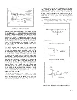
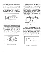
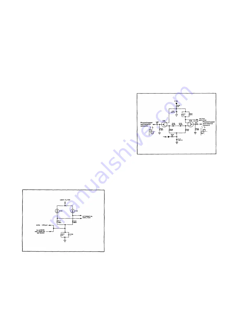
4-15. PHOTOCHOPPER AND BALANCE CIRCUIT (See
Figure 4-7). The Photochopper and Balance Circuit
algebraically sums the outputs of the Input Filter, Zero Circuit,
and Slidewire and Damping Network, and converts the
summation to 50 or 60 Hz form depending on the power line
frequency. Resistor R-119 sums the outputs from the Zero
Circuit and Slidewire and Damping Network. C-106
suppresses spurious voltages that may appear across R-119.
The voltage difference between the potential across R-119 and
the potential from the Input Filter is applied across the
photoconductive cells and their load resistors R-117 and
R-118. The photoconductive cells V-101 and V-102 are
alternately turned on and off by neon bulbs DS-2 and DS-4.
The bulbs are driven as described in Paragraph 4-22 in
synchronism with the power line. This switching action of the
photoconductive cells causes an ac error signal output whose
peak-to-peak amplitude is equal to the dc error signal. The ac
error signal will be either in phase or 180 degrees out of phase,
with respect to the power line, depending on the polarity of the
dc error signal. The direction of rotation of the servo motor is
determined by the relative phase excitation of the winding in
the servo amplifier's output Power Amplifier/Demodulator
Stage and the phase of the ac error signal. This phase
sensing causes the motor to drive potentiometer R-174 in a
direction necessary to seek balance. The total magnitude of
the error signal never exceeds 10 mv on the X-axis or 7 mv on
the Y-axis, and as the instruments must be sensitive to
approximately 0.1% of this voltage, it is apparent that error
signals present are exceedingly small, actually in the low
microvolt region. With this in mind, all input circuitry is carefully
engineered to minimize interference from stray hum pickup and
thermal emfs.
FIGURE 4-7. PHOTOCHOPPER AND
BALANCE CIRCUIT
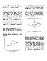
4-16. DIFFERENTIAL AMPLIFIER (See Figure 4-8). The ac
error signal from the Modulator and Balance Network is applied
to the Gates of Q-101 and Q-102 through coupling capacitors
C-109 and C-110. At time T1; a positive voltage is applied to
the Gate of Q-101, the Source will follow the Gate, and a
positive voltage appears at the Source of Q-102. This positive
voltage at the Source, together with the negative voltage at the
Gate, causes Q-102 to "shut-off" and the Drain becomes more
positive. At time T2, the Source-Gate junction of Q-102 to turn
on and the Drain will become more negative. Components R-
130, C-115, R-129, and C-114 are power supply filters.
Capacitors C-112 and C-113 couple the signal from Q-101 to
Q-102. Resistors R-128 and R-132 provide Source loads, and
R-131 provides the Drain load for Q-102. This stage has a
voltage gain of approximately ten.
FIGURE 4-8. DIFFERENTIAL AMPLIFIER
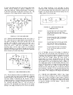
4-17. VOLTAGE AMPLIFIER (See Figure 4-9.) The ac error
signal from the Differential Amplifier is capacitor coupled by C-
116 to the base of the first transistor in the voltage amplifier, Q-
103. This high voltage gain section is comprised of three dc
coupled silicon transistors, Q-103, Q-104, and Q-105. This
stage has a minimum ac feedback of 20 db to insure stable
long term performance. The closed loop ac gain is dictated by
resistors R-136 and R-137. R-137 serves to vary the amount
of feedback and act as the servo amplifier gain control. The
electrical location of this control makes it suitable for physically
placing it with the low level dc circuitry and having no danger of
undesired feedback or oscillation. The dc stability of this stage
is achieved by the feedback path from the collector of Q-105.
This feedback path is a low pass filter comprised of resistors
R-138 and R-104, and capacitors C-118 and C-120. It
provides good dc negative feedback, but has adequate ac by-
passing so that it has no influence on the overall ac gain of the
amplifier. The several second warm-up time of the recorder is
caused by the time constant of this feedback network. Diode
CR-103 is used to improve the bias voltage conditions on the
input of Q-105 so that R-141 may be a reasonable size. R-139
4-4
Содержание HP-7035B
Страница 1: ...TECHNICAL MANUAL HEWLETT PACKARD MODEL HP 7035B ...
Страница 9: ...FIGURE 1 4 DIMENSION DRAWING FIGURE 1 5 ACCESSORIES 1 3 ...
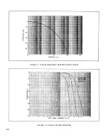
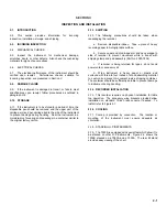
Страница 12: ...FIGURE 1 7 TYPICAL FREQUENCY RESPONSE INPUT FILTER FIGURE 1 8 TYPICAL DYNAMIC RESPONSE 1 6 ...
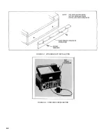
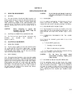
Страница 14: ...FIGURE 2 1 WING BRACKET INSTALLATION FIGURE 2 2 STACKED CONFIGURATION 2 2 ...
Страница 16: ...FIGURE 3 1 FRONT PANEL CONTROLS 7035B AND 7035B 001 MODELS 3 2 ...
Страница 20: ...FIGURE 4 1 BLOCK DIAGRAM FIGURE 4 2 DETAILED BLOCK DIAGRAM 4 2 ...
Страница 48: ...TM 11 6625 2850 14 P FIGURE 6 1 EXPLODED VIEW CABINET 6 9 ...
Страница 49: ...TM 11 6625 2850 14 P FIGURE 6 2 EXPLODED VIEW CARRIAGE ARM SHEET 1 OF 2 6 10 ...
Страница 58: ...FIGURE 7 1 COMPONENT IDENTIFICATION FRAME 7 8 ...
Страница 59: ...TM 11 6625 2850 14 P Figure 7 2 Component Identification Circuit Board 7 9 ...
Страница 60: ...TM 11 6625 2850 14 P Figure 7 3 Schematic Model 7035B D 07035 92550 7 10 ...
Страница 62: ...TM 11 6625 2850 14 P FIGURE 8 1 COMPONENT IDENTIFICATION CIRCUIT BOARD 8 2 ...
Страница 66: ...TM 11 6625 2850 14 P FIGURE 8 5 EXPLODED VIEW CARRIAGE ARM 8 6 ...

