TABLE 1-2. ACCESSORY SUPPLIES
1251-0293
Connector, Male, 24 pin
2110-0063
Fuse, 3/4 Amp (1)
(Mate to J-602)(1)
5080-7979
Pen, Disposable, Red Pack of 3 (1)
2110-0065
Fuse, 3/8 Amp (1)
5080-7980
Pen, Disposable, Blue Pack of 3 (1)
9270-1006
Graph Paper, English Calibrated
(Heavy) (10)
1540-0149
Plastic Box (1)
9270-1007
Graph Paper, English Calibrated
9220-1519
Filler Pad (1)
(Light) (10)
5080-3635
Slidewire Lubricant (1)
9270-1023
Graph Paper, Metric Caption-001,
Calibrated (Heavy) (10)
5080-3605
Slidewire Cleaner (1)
9270-1027
Graph Paper, Metric Caption-001,
8120-1378
Power Cord (1)
Calibrated (Light) (10)
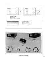
1-17. MODEL 7563A LOG VOLTMETER/ AMPLIFIER
1-18. The Model 7563A DC Log Voltmeter/Amplifier is
designed to perform two independent operations. As a
voltmeter, usable over a 110 dB input amplitude range,
accurate readings within 1.5 dB over an 80 dB dynamic range
are achieved, and the need for range switching is
unnecessary. As a log amplifier, output signals are
logarithmically related to applied input signals; this solid-state
amplifier permits semilogplotting operations with HP X-Y and
strip-chart recorders, and will operate with most other
recorders and oscilloscopes. Two amplifiers may be used for
log-log records.
1-19. MODEL 17108A TIME BASE
1-20. The 17108A is a self-contained external time base which
will operate on either axis of the 7035B. Any number of
recorders may be driven simultaneously providing the
combined parallel input impedance is 20, 000 ohms or more.
Five sweep speeds are provided from 0.5 to 50 seconds/inch.
1-21. MODEL 10025A STRAIGHT-THROUGH VOLTAGE
PROBE
1-22. The 10025A is a flexible probe with small, pushbutton
pincer jaws which provide a straight-through connection to the
7035B. Maximum input voltage is 600 volts peak. The cable is
terminated in a shielded dual banana plug.
1-23. MODEL 10111A ADAPTER
1-24. The 10111A (shielded banana-post-to-female-BNC)
converts banana post inputs on 7035B to shielded BNC inputs
for low-level signal work. This adapter may be used in pairs for
balanced input characteristics.
1-25. MODEL 10002A/B/C/D VOLTAGE DIVIDER PROBE.
1-26. The Voltage Divider Probe (50:1) extends the voltage
range of the 7035B to 1000 volts full scale. The high input
impedance (9 meg of this probe also reduces the loading of the
7035B on the system under test. Accuracy is ± 3%, requires
10111 Adapter, and not usable on the 1 mV/in. and 10 mV/in.
(0.4 mV/cm and 4 mV/cm) ranges. The length of the 10002A
is 5 feet, 10002B is 10 feet, 10002C is 5 feet with a black
identification boot, and the 10002C is 10 feet with a black
identification boot.
1-27. MODEL 11000A CABLE ASSEMBLY
1-28. Dual banana plugs terminate a section of 50-ohm cable,
44 inches overall, plugs for binding posts spaced 3/4 inch.
1-29. TYPICAL PERFORMANCE
1-30. INPUT RESISTANCE VS OFF BALANCE
CHARACTERISTICS
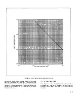
1-31. The input resistance is constant, regardless of off
balance condition except for the 1 mV/in. (0.4 mV/cm) range.
This range, operating in potentiometric mode, draws all the
current flowing in the balance loop through the input circuit.
Referring to Figure 1-6, observe that a linear relationship exists
between the distance off balance and the input resistance, and
because the input resistance at 1% of full scale off balance is
approximately 10 meg ohms, a small off balance condition is
noticeable.
1-32. NORMAL MODE NOISE
1-33. This instrument is designed to record dc signals.
Normal mode noise (like frequency) is often superimposed on
the low frequency, which if not eliminated, may produce
unsatisfactory recordings. An excessive amount of noise can
1-4
Содержание HP-7035B
Страница 1: ...TECHNICAL MANUAL HEWLETT PACKARD MODEL HP 7035B ...
Страница 9: ...FIGURE 1 4 DIMENSION DRAWING FIGURE 1 5 ACCESSORIES 1 3 ...
Страница 12: ...FIGURE 1 7 TYPICAL FREQUENCY RESPONSE INPUT FILTER FIGURE 1 8 TYPICAL DYNAMIC RESPONSE 1 6 ...
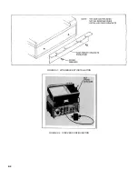
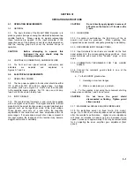
Страница 14: ...FIGURE 2 1 WING BRACKET INSTALLATION FIGURE 2 2 STACKED CONFIGURATION 2 2 ...
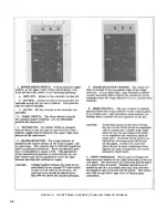
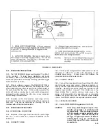
Страница 16: ...FIGURE 3 1 FRONT PANEL CONTROLS 7035B AND 7035B 001 MODELS 3 2 ...
Страница 20: ...FIGURE 4 1 BLOCK DIAGRAM FIGURE 4 2 DETAILED BLOCK DIAGRAM 4 2 ...
Страница 48: ...TM 11 6625 2850 14 P FIGURE 6 1 EXPLODED VIEW CABINET 6 9 ...
Страница 49: ...TM 11 6625 2850 14 P FIGURE 6 2 EXPLODED VIEW CARRIAGE ARM SHEET 1 OF 2 6 10 ...
Страница 58: ...FIGURE 7 1 COMPONENT IDENTIFICATION FRAME 7 8 ...
Страница 59: ...TM 11 6625 2850 14 P Figure 7 2 Component Identification Circuit Board 7 9 ...
Страница 60: ...TM 11 6625 2850 14 P Figure 7 3 Schematic Model 7035B D 07035 92550 7 10 ...
Страница 62: ...TM 11 6625 2850 14 P FIGURE 8 1 COMPONENT IDENTIFICATION CIRCUIT BOARD 8 2 ...
Страница 66: ...TM 11 6625 2850 14 P FIGURE 8 5 EXPLODED VIEW CARRIAGE ARM 8 6 ...


