


43
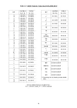
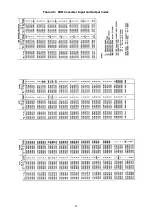
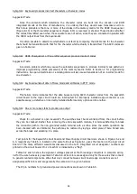
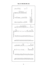
As an example, let us assume that the CQ key is to be coded with the three characters C, Q and a space.
Here is how we would fill in the chart:
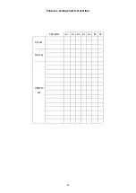
Character
A
0
A
1
A
2
A
3
A
4
A
5
A
6
C
1
1
0
0
0
0
1
CQ key
Q
1
0
0
0
1
0
1
SPACE
0
0
0
0
0
1
0
From Table 4.2, we see that the code for the first character, C, is 100 0011. Reversing the order, we
have 1100 001, which we enter in the first line of the coding chart. The code for Q is 101 0001. Reversing
the order, we have 1000 101, which we enter opposite the a in the chart. The space code is 010 0000,
which we reverse and enter opposite the "SPACE" row in the chart.
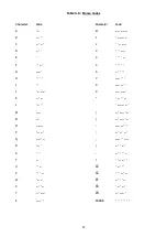
Note that in Table 4.2, there are two code columns for each character – a shifted and an unshifted one.
For the letter keys, these two codes are the same. For some keys, however, the shifted code is different,
and it produces a different character from the unshifted one. For example, the "1" key produces an
exclamation point if it is struck when one of the shift keys is held down. Similarly, the "2" key produces
quotation marks if the shift key is used.
Therefore, it is important to select the code from the correct column. If you want the identifier to
produce the character which appears on the lower half of the keytop, use the code from the "unshifted"
column. If you want the character appearing on the top half of the keytop, use the code from the "shifted"
column.
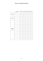
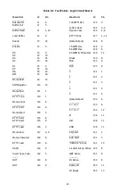
Now go through the table and place a large X in each square which contains a one, as shown in the
sample chart. These X's will correspond to the position of the diodes in the matrix on the logic board. Two
copies of Table 5.1 are included so that a different coding can be set up in the future.
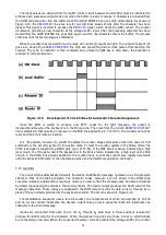
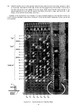
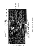
177. Check to make sure that the AC power cord has been disconnected from the outlet. Then remove the
logic circuit board from the bottom cover and position it on your work surface with the component
side up and the connector strip nearest you, The diode matrix will now be at the left edge of the
board and will be positioned as indicated by Figure 5.14.
178. The figure shows how the diodes should be positioned for the CQ key. Note that the diodes are
inserted into the board from the component side. Referring to the table you have prepared, install
diodes in the matrix at the appropriate positions. The diodes should be stood on end, with the
cathode end (the end to which the colored bands are closest) furthest from the surface of the board.
Be sure that the diode body is over the row of holes not connected by a conductor strip, as shown in
Figure 5.14. Solder the diode leads on the reverse side of the board and cut off excess leads.
179. Locate the jumper wire which was installed during initial assembly from a hole at the right edge of IC-
40 to one of the rows in the diode matrix. Disconnect the matrix end of the wire from the circuit
board. Note that a row of holes is provided along the right edge of the matrix, labeled with numbers 1
through 16 in Figure 5.14. Count the number of rows you have used for the HERE IS (identifier)
message, including any blanks or spaces. Add one to that number to obtain the number of the hole to
which the jumper should be connected. Then insert the free end of the jumper wire in the hole and
solder. As a double check, the jumper should be attached to a hole which is connected by a printed
conductor to the row of diode holes immediately following the last row of diodes you inserted in the
identifier portion of the matrix.
180. Reinstall the logic board on the bottom cover panel and secure it in place with four 6-32 keep nuts.
Be sure to put nylon washers on the screws at holes A and C as described in step 171. Reconnect the
AC power cord and switch the keyboard on, being careful not to touch exposed wiring. Wait a minute
for the sequencers to clear themselves. Check that the keyboard is still set to the Morse mode. Then
press the CQ key and check that the proper character sequence is transmitted. Do the same for the
AUX and HERE IS keys. If the message sequence is executed correctly, disconnect the AC cord. If not,
recheck the position and installation of all diodes. If correct, refer to the troubleshooting section of
this manual.
Содержание DKB-2010
Страница 1: ......
Страница 20: ...18...
Страница 39: ...37 Table 4 3 ROM Converter Input and Output Codes...
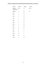
Страница 43: ...41 Table 5 1 Coding Chart for Identifier Character A0 A1 A2 A3 A4 A5 A6 CQ key AUX key HERE IS key...
Страница 44: ...42 Table 5 1 Coding Chart for Identifier Character A0 A1 A2 A3 A4 A5 A6 CQ key AUX key HERE IS key...
Страница 52: ...50 Figure 6 1 Logic Circuit Board Test Points...
Страница 53: ...51 Figure 6 2 Keyswitch Circuit Board Test Points...
Страница 54: ...52 Figure 6 3 Power Supply Circuit Board Test Points...
Страница 57: ...55 Table 6 4 DKB 2010 Wire List...
Страница 63: ...61...
Страница 64: ...62...
Страница 65: ...63...
Страница 67: ...65...
Страница 69: ...67...
Страница 71: ...69...
Страница 73: ...71...
Страница 75: ...73...
Страница 77: ...75...
Страница 79: ...77...
Страница 81: ...79...
Страница 83: ...81...
Страница 85: ...83...
Страница 87: ...85...
Страница 89: ...87...
Страница 91: ...89...
Страница 92: ...90...
Страница 93: ...91...
Страница 94: ...92...
Страница 95: ...93...
Страница 96: ...A1 EXTENDED MEMORY OPTION FOR THE DKB 2010 KEYBOARD INSTRUCTION MANUAL...
Страница 100: ...A5...
Страница 101: ...A6...