


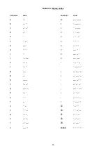


31
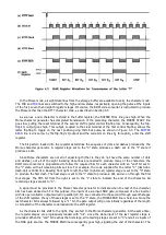
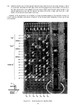
Figure 4.9 Suppression of Extra Dot to Produce Intercharacter Space
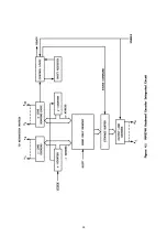
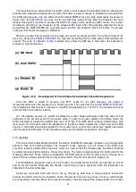
4.13 Morse Output Control
The Morse output control, shown in Figure 8.11, accepts inputs from the Morse character generator, the
BREAK key, and the RTTY character counter. It controls both the transmitter keying transistor and the
sidetone oscillator.
The MORSE CHARACTER line and the
MORSE END
line are applied to the inputs of a NAND gate (pins 9
and 10 of IC-18). During the production of character pulses, the
MORSE END
line remains high and the
pulses from the MORSE CHARACTER line appear inverted at the gate output. As explained in Section 4.12,
the
MORSE END
line goes low during the production of the dot which follows each character, resulting in an
intercharacter space.
The M/R bus and the BREAK line are applied to the two inputs of another NAND gate (pins 12 and 13 of
IC-55). Since the M/R bus is always high in the Morse mode, the output of the gate is low whenever the
BREAK key is pressed.
The outputs of the two gates are applied to the inputs of a third NAND gate (pins 1 and 2 of IC-18). If
either of the inputs is low, the output goes high. With the BREAK line low, the Morse character pulses
appear at the gate output. When the BREAK key is pressed , the gate output remains high regardless of the
incoming character pulses.
The output of the third gate drives the emitter of Q6, a constant current source, which in turn drives the
transmitter keying transistor, Q5. When the gate output is high, the keying transistor conducts. The tran-
sistor output may be connected for either cathode or grid-block keying, depending on which of the two
output jacks is used. For cathode keying, the cathode lead from the transmitter is connected to the collector
of Q5. The emitter is grounded through the grid-block jack. When the transistor is driven into conduction,
cathode current flows.
If the grid-block keying method is used, the transmitter's grid biasing circuit is connected to the emitter
keying transistor. The collector is grounded through the cathode jack. When the transistor conducts, it
shorts the bias source to ground.
A diode and capacitor are connected across the keying transistor to protect it from surges and the
application of reverse voltages.
The input signals also drive the sidetone oscillator through an inverter (part of IC-24) and a NAND gate
(pins 1-3 of IC-55) . The
RTTY TONE
bus, which originates in the RTTY character counter circuit (figure
8.9), is also applied to the gate input. If either the MORSE CHARACTER or BREAK line is high, or if the
RTTY
TONE
line is low, the gate output goes high. This signal is coupled to the input of another NAND gate (pin 4
of IC-55) which forms part of the sidetone oscillator. When the gate input is high, the oscillator is enabled.
Содержание DKB-2010
Страница 1: ......
Страница 20: ...18...
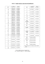
Страница 39: ...37 Table 4 3 ROM Converter Input and Output Codes...
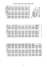
Страница 43: ...41 Table 5 1 Coding Chart for Identifier Character A0 A1 A2 A3 A4 A5 A6 CQ key AUX key HERE IS key...
Страница 44: ...42 Table 5 1 Coding Chart for Identifier Character A0 A1 A2 A3 A4 A5 A6 CQ key AUX key HERE IS key...
Страница 52: ...50 Figure 6 1 Logic Circuit Board Test Points...
Страница 53: ...51 Figure 6 2 Keyswitch Circuit Board Test Points...
Страница 54: ...52 Figure 6 3 Power Supply Circuit Board Test Points...
Страница 57: ...55 Table 6 4 DKB 2010 Wire List...
Страница 63: ...61...
Страница 64: ...62...
Страница 65: ...63...
Страница 67: ...65...
Страница 69: ...67...
Страница 71: ...69...
Страница 73: ...71...
Страница 75: ...73...
Страница 77: ...75...
Страница 79: ...77...
Страница 81: ...79...
Страница 83: ...81...
Страница 85: ...83...
Страница 87: ...85...
Страница 89: ...87...
Страница 91: ...89...
Страница 92: ...90...
Страница 93: ...91...
Страница 94: ...92...
Страница 95: ...93...
Страница 96: ...A1 EXTENDED MEMORY OPTION FOR THE DKB 2010 KEYBOARD INSTRUCTION MANUAL...
Страница 100: ...A5...
Страница 101: ...A6...