


28
Although the output of the RTTY timing chain is not used to clock the shift register in the Morse mode , VHØ
and HØ clock pulses are still needed in the keyencoder, buffer control, and RTTY loop interface circuits. The
M/R
bus is therefore connected through diode D8 to pin 8 of IC-35. With the mode switch set to the Morse
position, the gate input is pulled low, allowing the 60 WpM oscillator to drive the timing chain. As a result,
the required clock signals are produced.
Another inverter, part of IC-30, is used to invert the
BREAK
signal from the BREAK keyswitch. The output
is used in the RTTY encoder to interrupt the loop current and in the stage when the BREAK key is pressed.
4.11 RTTY Character Counter
When the keyboard is in the RTTY mode, a character counter keeps track of the number of characters
transmitted and warns the operator when the end of a line is approached. The counter is reset each time a
carriage return is transmitted, and is instructed not to count non-printing characters, When 64 printing
characters have been produced since the most recent carriage return, the counter output lights an indicator
lamp and triggers the sidetone oscillator to produce an audible warning.
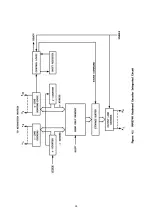
The counter, shown in Figure 8.9, consists of six flip-flops arranged as an ordinary binary counter, and a
control circuit. The clock signal is supplied from the RTTY control and decoding circuit (Figure 8.5) via the
RTTY LOAD line. Each time a character is loaded into the shift register, the counter increments, provided
that the D
7
data line from the ROM code converter is low. As discussed in Section 4.5, the D
7
line is low for
all printing characters, but is high for non-printing ones. The D
7
signal is applied to the J and K inputs of the
flip-flop, which toggles only when both input terminals are high.
The
D
6
line is high only for the carriage return character. When this character is loaded into the register,
both the D
6
line and the RTTY LOAD bus are high. These signals, applied to the inputs of a NAND gate (part
of IC-25), drive the gate output low, resetting all stages of the counter.
After 32 input pulses, the counter output goes high; after the 64th pulse it goes low again. The counter
output is fed to the clock input of another flip-flop (part of IC-23). When the counter completes its cycle, the
flip-flop toggles, driving the base of a PNP transistor, Q3, low. Since the emitter of the transistor is biased to
+5 Volt, the transistor conducts and the end-of-line warning lamp lights. The flip-flop's reset terminal is
connected to the output of the gate which drives the counter reset bus, so that the warning lamp is
extinguished when a carriage return is transmitted. The flip-flop's Q output is also coupled to the trigger
terminal of a monostable multivibrator (IC-13), The negative-going transition at the end of the 64th count
causes the monostable to toggle to the set state for a short period. The
RTTY TONE
line is driven low,
activating the sidetone oscillator (Figure 8.11) during the monostable period.
4.12 Morse Character Generator
The function of the Morse character generator, shown in Figure 8.10, is to convert the sequential output
bits from the shift register to a series of short and long pulses corresponding to the dots and dashes of
Morse code.
The cycle of operation is initiated when a character is transferred to the shift register from the storage
buffer. The
MORSE END
line, driven through an inverter from the shift register end-of-character sensing
circuit, goes high, setting the oscillator control flip-flop. The Q output of the flip-flop (pin 5 of IC-15) goes
high, driving the MORSE START line high and enabling a NAND gate which controls the Morse oscillator.
The oscillator, consisting of the NAND gate (part of IC-14) and two inverters, determines the Morse
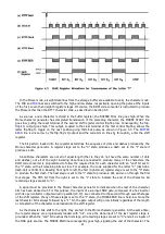
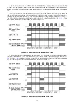
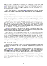
transmission rate. The oscillator frequency is controlled by the front-panel Morse speed control, P301. The
oscillator output is coupled to the input of a three-bit counter (IC-26); its inverted output is fed to the input
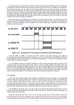
of the dot flip-flop (pit 5 of IC-23). The counter states are decoded by a 4-line-to-10-line decoder (IC-31) to
produce sequential pulses on its output lines, as shown in Figure 4.6 (for clarity, only the first four output
lines are shown).
Содержание DKB-2010
Страница 1: ......
Страница 20: ...18...
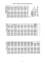
Страница 39: ...37 Table 4 3 ROM Converter Input and Output Codes...
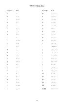
Страница 43: ...41 Table 5 1 Coding Chart for Identifier Character A0 A1 A2 A3 A4 A5 A6 CQ key AUX key HERE IS key...
Страница 44: ...42 Table 5 1 Coding Chart for Identifier Character A0 A1 A2 A3 A4 A5 A6 CQ key AUX key HERE IS key...
Страница 52: ...50 Figure 6 1 Logic Circuit Board Test Points...
Страница 53: ...51 Figure 6 2 Keyswitch Circuit Board Test Points...
Страница 54: ...52 Figure 6 3 Power Supply Circuit Board Test Points...
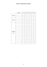
Страница 57: ...55 Table 6 4 DKB 2010 Wire List...
Страница 63: ...61...
Страница 64: ...62...
Страница 65: ...63...
Страница 67: ...65...
Страница 69: ...67...
Страница 71: ...69...
Страница 73: ...71...
Страница 75: ...73...
Страница 77: ...75...
Страница 79: ...77...
Страница 81: ...79...
Страница 83: ...81...
Страница 85: ...83...
Страница 87: ...85...
Страница 89: ...87...
Страница 91: ...89...
Страница 92: ...90...
Страница 93: ...91...
Страница 94: ...92...
Страница 95: ...93...
Страница 96: ...A1 EXTENDED MEMORY OPTION FOR THE DKB 2010 KEYBOARD INSTRUCTION MANUAL...
Страница 100: ...A5...
Страница 101: ...A6...