


MPC5553/MPC5554 Microcontroller Reference Manual, Rev. 5
Freescale Semiconductor
2-35
4
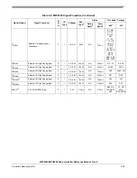
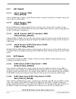
The pad type is indicated by one of the abbreviations; F for fast, MH for medium (high voltage), SH for slow (high voltage), A for analog, AE for
analog with ESD protection circuitry. Some pads may have two types, depending on which pad function is selected.
5
The Status During Reset pin is sampled after the internal POR is negated. Prior to exiting POR, the signal has a high impedance.
Terminology is O — output, I — input, up — weak pullup enabled, down — weak pulldown enabled, low — output driven low, High — output driven
high. A dash on the left side of the slash denotes that both the input and output buffers for the pin are off. A dash on the right side of the slash
denotes that there is no weak pull up/down enabled on the pin. The signal name to the left or right of the slash indicates the pin is enabled.
6
Function after reset of GPI is general-purpose input. A dash on the left side of the slash denotes that both the input and output buffers for the pin
are off. A dash on the right side of the slash denotes that there is no weak pull up/down enabled on the pin.
7
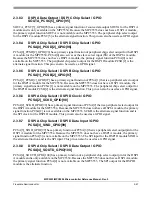
The 496 assembly contains the VertiCal base and includes all of the 416 package pins.
8
The EBI is specified and tested at 1.8 V and 3.3 V.
9
To provide more flexibility in configuring the device, the ADDR[8:11] pins are muxed to several signal functions, such as the primary function in
ADDR[8:31]_GPIO[4:27] and the alternate function in signal CS[0:3]_ADDR[8:11]_GPIO[0:3]. Only configure one set of ADDR[8:11] pins for the
address input.
10
The function and state of this pin after execution of the BAM program is determined by the BOOTCFG[0:1] pins. Refer to
for detail on
the external bus interface (EBI) configuration after execution of the BAM program.
11
Although GPIO versus EBI function is specified in the SIU, when EBI function is chosen, the function must also be enabled in the EBI for these
pins. The SIU and EBI configurations must match for proper operation.
12
The active function for the WE/BE[0:3]_GPIO[64:65] is specified in the PA field of the SIU_PCR register. When configured for WE/BE[0:3], specify
the write enable or byte enable operation in the EBI_BR0 through EBI_BR3 registers.
13
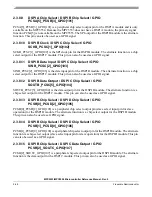
MCKO is only enabled if debug mode is enabled. Debug mode can be enabled before or after exiting System Reset (RSTOUT negated).
14
MDO[0] is driven high following a power-on reset until the system clock achieves lock, at which time it is then negated. There is an internal pull
up on MDO[0].
15
The function of the MDO[11:4]_GPIO[82:75] pins is selected during a debug port reset by the EVTI pin or by selecting FPM in the NPC_PCR.
When functioning as MDO[11:4] the pad configuration specified by the SIU does not apply.
16
The pullup on TDO is only functional when not in JTAG mode, that is with JCOMP negated.
17
The function and state of the FlexCAN A and eSCI A pins after execution of the BAM program is determined by the BOOTCFG[0:1] pins. Refer
to
for detail on the FlexCAN and eSCI pin configuration after execution of the BAM program.
18
All analog input channels are connected to both ADC blocks. These pins must only use an ESD rail supply.
19
Because the primary signal function designations for the analog functions AN[12] through AN[15] are internally reserved, the PA field of the
corresponding SIU_PCR register must be set to the Main Primary function value of 0b011 to use analog functions AN[12] through AN[15].
20
To use the Serial Data Strobe functions, the PA fields of the corresponding SIU_PCR registers must be set to the GPIO setting of 0b00. Because
SDS, SDO, SDI, and FCK use the GPIO setting, a G is shown in the P/A/G column. However, these signals do not support true GPIO functionality.
21
If the analog features are used, tie V
DDEH9
to V
DDA1
.
22
Because other balls already are named EMIOS[14:15], the balls for these signals are named GPIO[203:204].
23
The GPIO[205] pin is a protect-for pin for configuring an external boot for a double data rate (DDR) memory.
24
The GPIO[206:207] pins are protect-for pins for double data rate memory data strobes.
25
GPIO[206:207] can be selected as the source for the eQADC trigger in the eQADC Trigger Input Select Register (SIU_ETISR).
26
The function after reset of the XTAL pin is determined by the value of the signal on the PLLCFG[1] pin. When bypass mode is chosen, XTAL has
no function and must be grounded.
27
When the FMPLL is configured for external reference mode, the V
DDE5
supply affects the acceptable signal levels for the external reference.
Refer to
Section 11.1.4.2, “External Reference Mode
.”
28
The function after reset of the EXTAL_EXTCLK pin is determined by the value of the signal on the PLLCFG[0:1] pins. If the EXTCLK function is
chosen, the valid operating voltage for the pin is 1.6–3.6 V. If the EXTAL function is chosen, the valid operating voltage is 3.3 V. Refer to
29
V
RC33
is the 3.3 V input for the voltage regulator control.
30
V
RCVSS
is connected internally to V
SSSYN
.
31
The V
DDAn
and V
SSAn
supply inputs are separate traces in the package substrate. Each trace is bonded to a separate pad location, which
provides isolation between the analog and digital sections within each ADC.
32
V
PP
can be tied to 5.0 V for both the read operation and program/erase operation.
33
If the battery backed SRAM is not used, tie the V
STBY
pin to V
SS
ground.
34
The V
DDEH9
segment can be powered from 3.0–5.0 V for mux addressing or SSI functions, but must meet the V
DDA1
specifications of 4.5 V to
5.25 V for analog input function.
35
All pins with pad type F are driven to the high state if their V
DDE
segment is powered on before V
DD33
.
36
The No Connect (NC) pins are reserved for the clock and inverted clock outputs for the DDR memory interface. In the MPC5554 416-pin package,
the two No Connect (NC) pins are isolated (not shorted together in the package substrate).
Содержание MPC5553
Страница 5: ...MPC5553 MPC5554 Microcontroller Reference Manual Rev 5 2 Freescale Semiconductor...
Страница 21: ...MPC5553 MPC5554 Microcontroller Reference Manual Rev 5 xvi Freescale Semiconductor...
Страница 47: ...MPC5553 MPC5554 Microcontroller Reference Manual Rev 5 1 26 Freescale Semiconductor...
Страница 163: ...MPC5553 MPC5554 Microcontroller Reference Manual Rev 5 4 20 Freescale Semiconductor...
Страница 179: ...MPC5553 MPC5554 Microcontroller Reference Manual Rev 5 5 16 Freescale Semiconductor...
Страница 561: ...MPC5553 MPC5554 Microcontroller Reference Manual Rev 5 13 38 Freescale Semiconductor...
Страница 615: ...MPC5553 MPC5554 Microcontroller Reference Manual Rev 5 14 54 Freescale Semiconductor...
Страница 707: ...MPC5553 MPC5554 Microcontroller Reference Manual Rev 5 17 68 Freescale Semiconductor...
Страница 755: ...MPC5553 MPC5554 Microcontroller Reference Manual Rev 5 18 48 Freescale Semiconductor...
Страница 873: ...MPC5553 MPC5554 Microcontroller Reference Manual Rev 5 19 118 Freescale Semiconductor...
Страница 984: ...MPC5553 MPC5554 Microcontroller Reference Manual Rev 5 Freescale Semiconductor 21 41...
Страница 985: ...MPC5553 MPC5554 Microcontroller Reference Manual Rev 5 21 42 Freescale Semiconductor...
Страница 1019: ...MPC5553 MPC5554 Microcontroller Reference Manual Rev 5 22 34 Freescale Semiconductor...
Страница 1129: ...MPC5553 MPC5554 Microcontroller Reference Manual Rev 5 25 90 Freescale Semiconductor...
Страница 1207: ...Revision History 4 Freescale Semiconductor...


