


MPC5553/MPC5554 Microcontroller Reference Manual, Rev. 5
25-6
Freescale Semiconductor
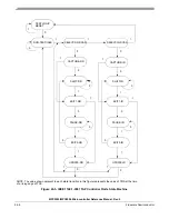
25.2.1.3
Message Data Out (MDO[3:0/11:0])
Message data out (MDO) are output pins used for uploading OTM, BTM, DTM, and other messages to
the development tool. The development tool should sample MDO on the rising edge of MCKO. The width
of the MDO bus used is determined by the Nexus PCR[FPM] configuration.
Following a power-on reset, MDO0 remains asserted until power-on reset is exited and the system clock
achieves lock.
25.2.1.4
Message Start/End Out (MSEO[1:0])
MSEO[1:0] are output pins that indicates when a message on the MDO pins has started, when a variable
length packet has ended, or when the message has ended. The development tool should sample the MSEO
pins on the rising edge of MCKO.
25.2.1.5
Ready (RDY)
RDY is an output pin that indicates when a device is ready for the next access.
25.2.1.6
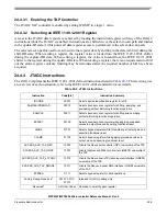
JTAG Compliancy (JCOMP)
The JCOMP signal enables or disables the TAP controller. The TAP controller is enabled when JCOMP
asserted, otherwise the TAP controller remains in reset.
25.2.1.7
Test Data Output (TDO)
The TDO pin transmits serial output for instructions and data. TDO is tri-stateable and is actively driven
in the SHIFT-IR and SHIFT-DR controller states. TDO is updated on the falling edge of TCK and sampled
by the development tool on the rising edge of TCK.
25.2.1.8
Test Clock Input (TCK)
The TCK pin is used to synchronize the test logic and control register access through the JTAG port.
25.2.1.9
Test Data Input (TDI)
The TDI pin receives serial test instruction and data. TDI is sampled on the rising edge of TCK.
25.2.1.10 Test Mode Select (TMS)
The TMS pin is used to sequence the IEEE
1149.1-2001 TAP controller state machine. TMS is sampled
on the rising edge of TCK.
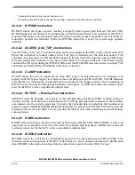
25.3
Memory Map
The NDI block contains no memory mapped registers. Nexus registers are accessed by the development
tool via the JTAG port using a register index and a client select value. The client select is controlled by
loading the correct access instruction into the JTAG controller; refer to
accessed by loading the appropriate value in the RS[0:6] field of the OnCE command register (OCMD)
via the JTAG port.
Содержание MPC5553
Страница 5: ...MPC5553 MPC5554 Microcontroller Reference Manual Rev 5 2 Freescale Semiconductor...
Страница 21: ...MPC5553 MPC5554 Microcontroller Reference Manual Rev 5 xvi Freescale Semiconductor...
Страница 47: ...MPC5553 MPC5554 Microcontroller Reference Manual Rev 5 1 26 Freescale Semiconductor...
Страница 163: ...MPC5553 MPC5554 Microcontroller Reference Manual Rev 5 4 20 Freescale Semiconductor...
Страница 179: ...MPC5553 MPC5554 Microcontroller Reference Manual Rev 5 5 16 Freescale Semiconductor...
Страница 561: ...MPC5553 MPC5554 Microcontroller Reference Manual Rev 5 13 38 Freescale Semiconductor...
Страница 615: ...MPC5553 MPC5554 Microcontroller Reference Manual Rev 5 14 54 Freescale Semiconductor...
Страница 707: ...MPC5553 MPC5554 Microcontroller Reference Manual Rev 5 17 68 Freescale Semiconductor...
Страница 755: ...MPC5553 MPC5554 Microcontroller Reference Manual Rev 5 18 48 Freescale Semiconductor...
Страница 873: ...MPC5553 MPC5554 Microcontroller Reference Manual Rev 5 19 118 Freescale Semiconductor...
Страница 984: ...MPC5553 MPC5554 Microcontroller Reference Manual Rev 5 Freescale Semiconductor 21 41...
Страница 985: ...MPC5553 MPC5554 Microcontroller Reference Manual Rev 5 21 42 Freescale Semiconductor...
Страница 1019: ...MPC5553 MPC5554 Microcontroller Reference Manual Rev 5 22 34 Freescale Semiconductor...
Страница 1129: ...MPC5553 MPC5554 Microcontroller Reference Manual Rev 5 25 90 Freescale Semiconductor...
Страница 1207: ...Revision History 4 Freescale Semiconductor...


