RIGENERATIVE
SINUS PENTA
APPLICATION
94/
140
0
1
2
3
4
0
1
2
3
4
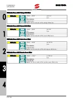
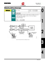
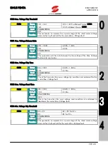
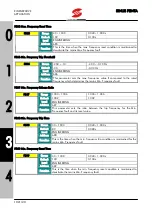
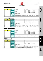
P535a/b/c Phase A/B/C Voltage RMS Offset
P535a/b/c
Range
–2048
÷
+2047
±
47.4 V
Default
0
0 V
Level
ENGINEERING
Address
970/971/972
Function
Register for the correction of the voltage offset error.
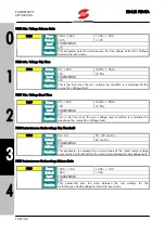
P536a/b/c Phase A/B/C Current RMS Offset
P536a/b/c
Range
–2048
÷
+2047
±
0.3 %
Default
0 %
0 %
Level
ENGINEERING
Address
973/974/975
Function
Register for the correction of the current offset error.
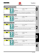
P537a/b/c Phase A/B/C Active Power Offset
P537a/b/c
Range
–2048
÷
+2047
±
0.015 %
Default
0
0 %
Level
ENGINEERING
Address
976/977/978
Function
Register for the correction of the active power offset error.
P538a/b/c Phase A/B/C Reactive Power Offset
P538a/b/c
Range
–2048
÷
+2047
±
0.015 %
Default
0
0 %
Level
ENGINEERING
Address
979/980/981
Function
Register for the correction of the reactive power offset error.


