SINUS PENTA
REGENERATIVE
APPLICATION
93/
140
0
1
2
3
4
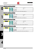
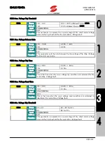
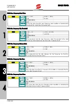
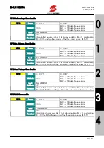
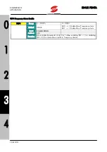
P531a/b/c Phase A/B/C Voltage RMS Gain
P531a/b/c
Range
–2048
÷
+2047
1
±
50%
Default
0
1
Level
ENGINEERING
Address
958/959/960
Function
This gain affects both the voltage RMS value and the apparent power RMS
value.
V=V*(1+(P531/212))
The overall calibration range is then 1
±
50%.
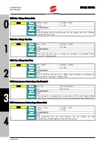
P532a/b/c Phase A/B/C Current RMS Gain
P532a/b/c
Range
–2048
÷
+2047
1
±
50%
Default
0
1
Level
ENGINEERING
Address
961/962/963
Function
This gain affects both the current RMS value and the apparent power RMS
value.
I=I*(1+(P532/212))
The overall calibration range is then 1
±
50%.
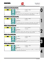
P533a/b/c Phase A/B/C Active Power Gain
P533a/b/c
Range
–2048
÷
+2047
1
±
50%
Default
0
1
Level
ENGINEERING
Address
964/965/966
Function
This register calibrates the calculation of Active Power P.
P=P*(1+(P533/212))
The overall calibration range is then 1
±
50%.
P534a/b/c Phase A/B/C Reactive Power Gain
P534a/b/c
Range
–2048
÷
+2047
1
±
50%
Default
0
1
Level
ENGINEERING
Address
967/968/969
Function
This register calibrates the calculation of Reactive Power Q.
Q=Q*(1+(P534/212))
The overall calibration range is then 1
±
50%.


