V&T Technologies Co., Ltd.
http://www.ecodrivecn.com
Chapter 6 Parameter Description
73
It is the process open loop operation and process close loop operation switching terminal. When this
terminal is enabled, it means process close loop operation and when the terminal is disable, it means
process open loop operation.
52: Main frequency source switching to digital voltage reference
53: Reserved
54: Main frequency source switching to AI1
55: Main frequency source switching to AI2
56~57: Reserved
The above three functions are set to facilitate the switching of main frequency source. When the terminal
is switching from disabled status to enabled status, The edge trigger is valid. When this terminal is
enabled, it will switch from the current main frequency source mode to the main frequency source mode
corresponding to this terminal function.
58: Auxiliary frequency source switching to disabled
59: Reserved
60: Auxiliary frequency source switching to AI1
61: Auxiliary frequency source switching to AI2
62~66: Reserved
67: Closed loop output forced to be 0
Under process closed loop control, when the terminal is valid, the output frequency of the inverter
process closed loop adjustment is forced to set as 0.
68: PID positive or negative function
PID is positeve function at default. It should enable negative function when feedback value is greater
than reference value and the frequency needed increase. This function can realized through setting
P8.09=1 or multi
−
function terminal function setting as 68.
Note:
◆
P8.09=0, Terminal function is invalid: Positive;
◆
P8.09=1, Terminal function is valid: Positive;
◆
P8.09=1, Terminal function is invalid: Negative;
◆
P8.09=0
,
Terminal function is valid: Negative.
69~98: Reserved.
It can properly enlarge the setup value of P5.07 to improve the anti
−
interference capability of the terminal.
The longer the terminal filter time is, the longer the delay time of the terminal action is.
The X1 and X2 terminal with delay input signal function once receive valid signal change. When the
inverter need delay a certain time after receive input terminal signal, this functional code can realized.
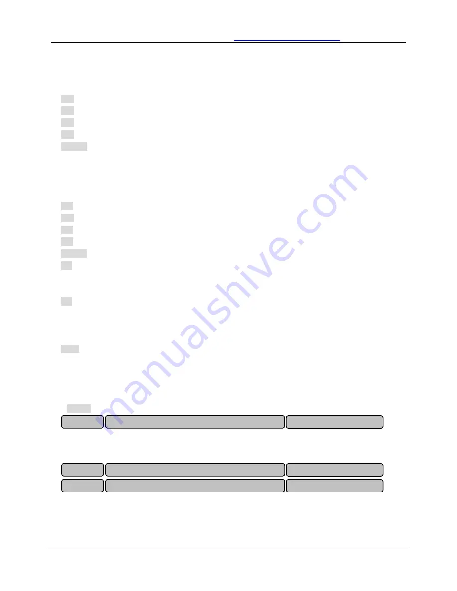
P5.07
X1 to X4 terminal filtering time
0.000~1.000 s (0.001s)
P5.10
X1 terminal delay time
0.0~ 999.9 s (0.0s)
P5.10
X2 terminal delay time
0.0~ 999.9 s (0.0s)


