408
32072H–AVR32–10/2012
AT32UC3A3
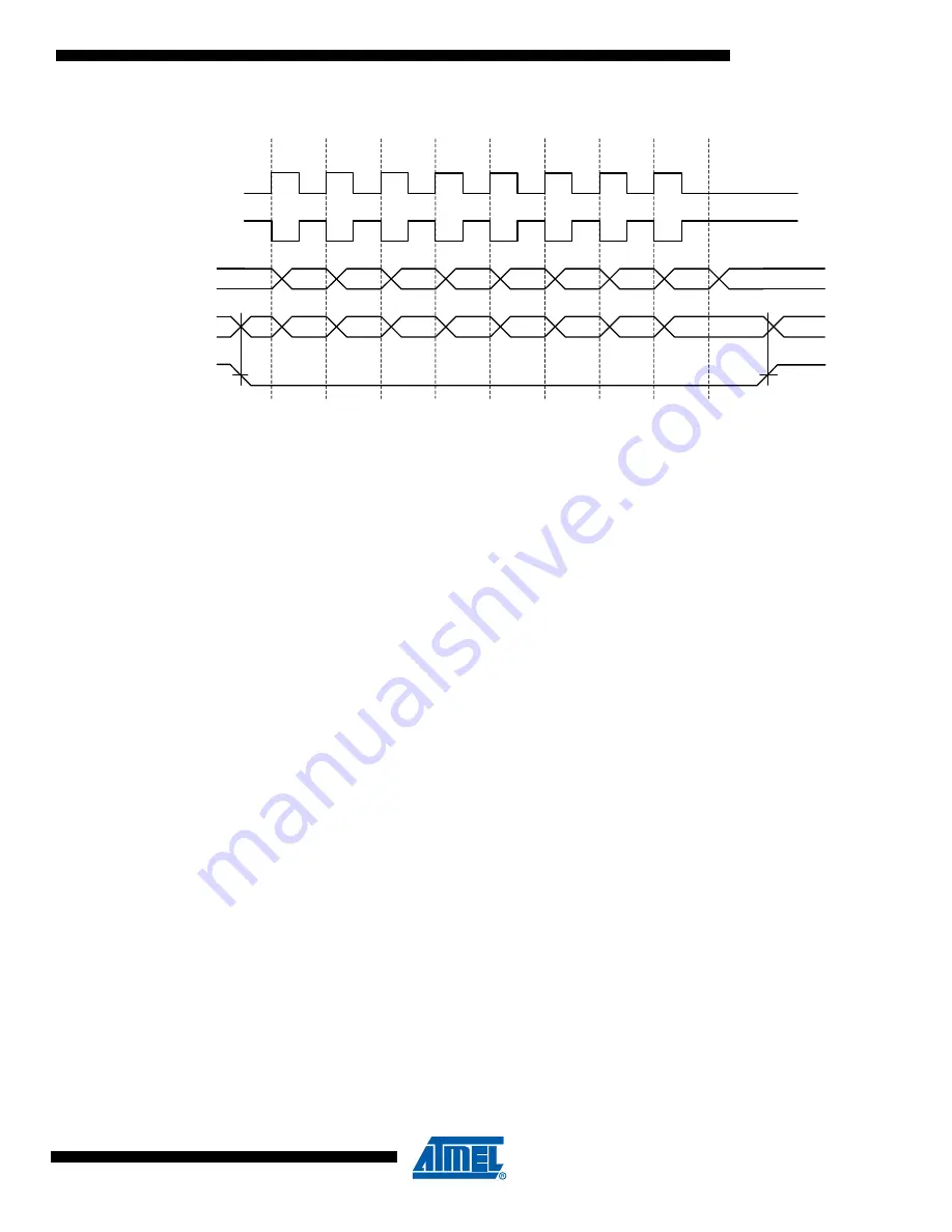
Figure 21-4. SPI Transfer Format (NCPHA = 0, 8 bits per transfer)
21.7.3
Master Mode Operations
When configured in master mode, the SPI uses the internal programmable baud rate generator
as clock source. It fully controls the data transfers to and from the slave(s) connected to the SPI
bus. The SPI drives the chip select line to the slave and the serial clock signal (SPCK).
The SPI features two holding registers, the Transmit Data Register (TDR) and the Receive Data
Register (RDR), and a single Shift Register. The holding registers maintain the data flow at a
constant rate.
After enabling the SPI, a data transfer begins when the processor writes to the TDR register.
The written data is immediately transferred in the Shift Register and transfer on the SPI bus
starts. While the data in the Shift Register is shifted on the MOSI line, the MISO line is sampled
and shifted in the Shift Register. Transmission cannot occur without reception.
Before writing to the TDR, the Peripheral Chip Select field in TDR (TDR.PCS) must be written in
order to select a slave.
If new data is written to TDR during the transfer, it stays in it until the current transfer is com-
pleted. Then, the received data is transferred from the Shift Register to RDR, the data in TDR is
loaded in the Shift Register and a new transfer starts.
The transfer of a data written in TDR in the Shift Register is indicated by the Transmit Data Reg-
ister Empty bit in the Status Register (SR.TDRE). When new data is written in TDR, this bit is
cleared. The SR.TDRE bit is used to trigger the Transmit Peripheral DMA Controller channel.
The end of transfer is indicated by the Transmission Registers Empty bit in the SR register
(SR.TXEMPTY). If a transfer delay (CSRn.DLYBCT) is greater than zero for the last transfer,
SR.TXEMPTY is set after the completion of said delay. The CLK_SPI can be switched off at this
time.
During reception, received data are transferred from the Shift Register to the reception FIFO.
The FIFO can contain up to 4 characters (both Receive Data and Peripheral Chip Select fields).
While a character of the FIFO is unread, the Receive Data Register Full bit in SR remains high
(SR.RDRF). Characters are read through the RDR register. If the four characters stored in the
FIFO are not read and if a new character is stored, this sets the Overrun Error Status bit in the
SR register (SR.OVRES). The procedure to follow in such a case is described in
1
4
3
2
5
8
7
6
SPCK cycle (for reference)
SPCK
(CPOL = 0)
NSS
(to slave)
MISO
(from slave)
MOSI
(from master)
SPCK
(CPOL = 1)
MSB
6
4
5
LSB
1
2
3
6
LSB
1
2
3
4
5
*** Not Defined, but normaly LSB of previous character transmitted
MSB
***
Содержание AT32UC3A3128
Страница 61: ...61 32072H AVR32 10 2012 AT32UC3A3 PLLEN PLL Enable 0 PLL is disabled 1 PLL is enabled...
Страница 260: ...260 32072H AVR32 10 2012 AT32UC3A3 5 2560 3071 6 3072 3583 7 3584 4095 Bit Index n Sector Boundaries...
Страница 592: ...592 32072H AVR32 10 2012 AT32UC3A3 Manchester Configuration Register on page 614...
Страница 989: ...989 32072H AVR32 10 2012 AT32UC3A3 37 2 Package Drawings Figure 37 1 TFBGA 144 package drawing...
Страница 991: ...991 32072H AVR32 10 2012 AT32UC3A3 Figure 37 3 VFBGA 100 package drawing...


