


Operating
lnstructions-7D14
but
where the
signal is
sufficiently larger than
the
P-P
VOLTS
setting to
ensure a
steady count. Generally, begin
with
the largest
P-P
VOLTS setting. Then decrease
the
switch
setting if
necessary to
obtain
a
steady
count.
The
COUPLING
switch
determines the coupling be
tween
the
CH
A
INPUT
connector and
the trigger circuit.
Generally,
use AC coupling
to block the
DC
component
of
a
signal.
Otherwise, the DC component might cause the
signal
level
to
be beyond
the range of
the
LEVEL/SLOPE
control.
DC
coupling
can
be used
for
low-frequency signals,
or
for
pulses
with
known
DC levels.
See Table
1-1
in
the
Specification section
for
the
frequency range and amplitude
limits
for each
coupling method. The COUPLING switch
does not affect signals selected via the TRIG SOURCE
posi
tion
of
the
INPUT SENS
switch.
The
BW
switch
provides
a
means of filtering out high-
frequency noise
pulses
which
may
cause erratic readings.
Generally,
use
the 5 MHz setting unless the signal
to
be
counted
is above
this
frequency. The BW switch affects
signals
connected through both the
internal
TRIG
SOURCE
and
the
CH A
INPUT
connector.
The
trigger
circuit
has a
hysteresis (basic
sensitivity)
of
approximately
100
millivolts.
A typical signal waveform
at
the
input
to
the
trigger is
shown in
Fig. 2-3A.
The
hysteresis
of
the
trigger
is
represented
by
the shaded
area.
Each
time
the
signal
level
(including
DC level)
rises
above
the
upper
hysteresis
limit
e
2
,
and
falls below
the
lower
hysteresis limit e1,
the
trigger circuit
produces
a rectangular
waveform
as shown in Fig.
2-3B.
This
rectangular
waveform
is
the signal actually
counted by the
counting circuits.
Generally,
the
best
point
on
a
waveform
for
triggering
the
counter
is
where
the
slope is
steep, and therefore
usually
free of
noise
Assuming
a
sine-wave
signal
wave
form, the
steepest slope
occurs
at
the
zero-crossing
point.
Fig. 2-3. (A) Signal input to trigger; shaded area represents trigger
hysteresis
with PRESET button depressed. (B) Trigger output.
This
is
the point
on
the positive-going slope
selected for
triggering when
the
PRESET pushbutton
is
pressed, and is
the
condition
represented
in Fig. 2-3A and B.
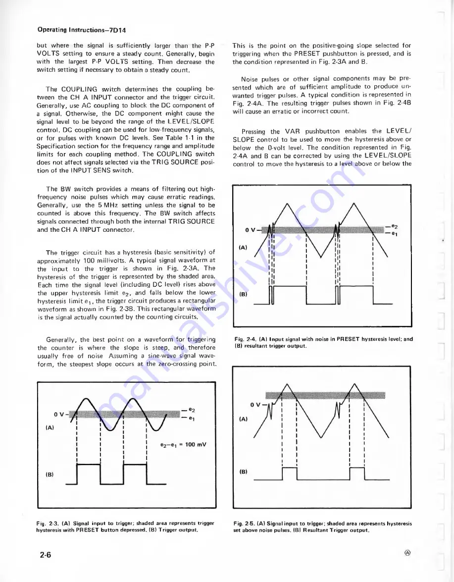
Noise
pulses or other signal components may be
pre
sented
which are of sufficient
amplitude to produce un
wanted
trigger
pulses. A typical
condition is represented in
Fig. 2-4A. The
resulting trigger pulses shown in Fig. 2-4B
will cause an
erratic
or incorrect
count.
Pressing
the
VAR pushbutton enables the
LEVEL/
SLOPE control
to
be used to move the hysteresis above or
below
the
0-volt
level.
The
condition represented
in
Fig.
2-4A
and B can be
corrected by using the LEVEL/SLOPE
control
to
move the hysteresis to a level above or below the
Fig.
2-4. (A) Input signal with noise in PRESET hysteresis level; and
(B)
resultant
trigger output.
Fig.
2-5. (A)
Signal
input to trigger; shaded
area represents hysteresis
set
above noise pulses. (Bl
Resultant Trigger output.
2-6
Summary of Contents for 7D14
Page 4: ...7D14 ...
Page 11: ...Operating Instructions 7D14 Fig 2 1 7D14 front panel controls and connectors 2 2 ...
Page 33: ... 3 13 Fig 3 11 Logic diagram for Zero Cancel Logic stage Circuit Description 7D14 ...
Page 38: ...3 18 Fig 3 16 Time Base and Control circuit detailed block diagram Circuit Description 7D14 ...
Page 44: ...NOTES ...
Page 46: ...NJ Fig 4 1 Electrode configuration for semiconductors in this instrument I ...
Page 68: ...NOTES ...
Page 96: ... 7DI 4 DIGITAL COUNTER UNIT ...
Page 98: ...GRS 0371 BLOCK DIAGRAM ...
Page 99: ......
Page 103: ...0 0 I 200 mV 500 µs 0 001 200 mV 500 µs 0 001 MHz 00 mV E 00 µs 0 001 MHz ...
Page 106: ...1 ...
Page 110: ...A2 Logic Circuit Board Assembly jQ798i 798 jc743 CR744t uni R724 R742 JL744S FrR796 ...
Page 113: ......
Page 114: ...P 0 A2 LOGIC BOARD ...
Page 121: ... A B D t F H J NPR Tj ZWX V A AC M AEA HUM qAZ DEF HJ N P R S T J V V7X y ABM APAI AA 7DI4 ...
Page 129: ......
Page 130: ...4 7D14 DIGITAL COUNTER ...


