


VXIbus Interface
7
7
Protocol/Signal
Reg,
lower
1
1
1
1
1
1
1
1
8148
Protocol/Signal
Reg,
upper
0
0
0
1
1
0
1
1
8149
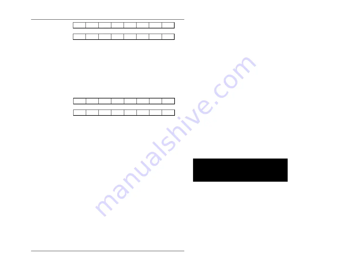
A read of this register reads the protocol register; a write writes the signal register.
The protocol register (the read value) defines the EPC-7 as being a servant and
commander, having a signal register, being a bus master and an interrupter, providing
the shared-memory protocol, and not providing fast handshake mode.
When written from the VXIbus, this register is the signal register. The value written
enters the signal FIFO (two deep) or returns a bus error (BERR) if the FIFO is
already full.
Response Register, lower
LOCK
1
ABMH
SIG
MLCK
WRCP
FSIG
LSIG
814A
Response Register, upper
0
1
DOR
DIR
ERR
RRDY
WRDY
1
814B
This register contains some VXI-defined state bits associated with message handling,
and several EPC-7 dependent bits.
DOR
RAM bit available to software for VXI communication protocols.
DIR
RAM bit available to software for VXI communication protocols.
ERR
RAM bit available to software for VXI communication protocols.
RRDY Read ready. A 1 denotes that the message registers contain outgoing data to
be read by another device. RRDY is cleared when the message low register
is read.
WRDY Write ready. If set, the message registers are armed for an incoming mes-
sage. When a write occurs into the message-low register, WRDY is cleared
and the MSGR interrupt condition is asserted.
LOCK RAM bit available to software.
ABMH This EPC-7 specific bit is cleared when the message high register is read or
written from the VXIbus. It serves as a location monitor for determining
whether a message is 16 or 32 bits in length.
SIG
If this EPC-7 specific bit is 0, the signal register FIFO is empty.
Page 57
Artisan Technology Group - Quality Instrumentation ... Guaranteed | (888) 88-SOURCE | www.artisantg.com