250
6.2.4.
Picture Signal Scanning Block
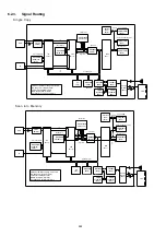
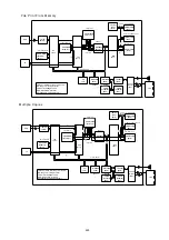
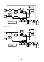
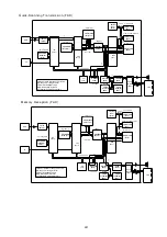
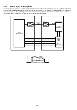
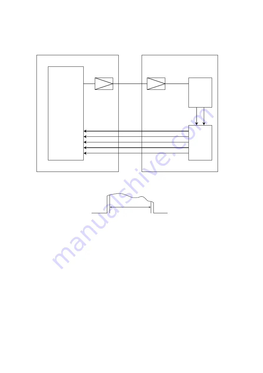
The image data read by the optical unit is input to the CCD mounted on the CCD PC Board, then transferred to the FCB PC Board
after the optical information is converted into an electrical signal by the CCD. The following shows a block diagram of the picture
signal scanning circuit. This picture signal scanning circuit consists of (1) ABC circuit, (2) shading correction circuit, (3) offset con-
trol circuit, (4) picture signal binary coding correction circuit and (5) reducing circuit.
W
B
ADIN1
2048 bit
Effective Scan Width
CCD
uPD3734ACY
IC160
MN86075
CCD
Drive
Circuit
IC140
DZZAC000168
VIDEO
(odd)
ADIN1
(2)(3)(4)(5)
(1)
Summary of Contents for Panafax DX-2000
Page 2: ......
Page 27: ...27 9 1 Screw 19 10 Release two Latch Hooks 11 Remove the SNS Assembly 121 9 10 11 ...
Page 49: ...49 2 15 Screw Identification Template ...
Page 57: ...57 3 7 3 Option Cassette Circuit 555 748 728 744 928 953 730 731 731 952 944 930 931 931 ...
Page 58: ...58 3 7 4 LAN Control Circuit 522 CN50 1102 1104 1101 N C N C RD N C N C RD TD TD ...
Page 59: ...59 3 7 5 Page Description Language Printer Interface Kit ...

